 ChipApex | Global Electronic Components Supplier
9DB801CFLF
Search Product
Search Post
— IC芯片 | 连接器 | 传感器 | 被动器件 —
Search productSearch post
— IC芯片 | 连接器 | 传感器 | 被动器件 —
Consult the customer manager about the wholesale price.
consultation hotline:86-132-6715-2157
email:[email protected]
Contact the product manager for consultation. One-stop consultation is available.
Do you want a lower wholesale price? Please send us your inquiry and we will reply immediately.
The Renesas Electronics Corporation 9DB801CFLF is a PCI Express zero-delay buffer IC designed for high-speed clock distribution. It features one differential input and eight differential outputs, operating at frequencies up to 400 MHz. The device supports HCSL input signaling and provides HCSL or LVDS output options. It functions within a supply voltage range of 3.135 V to 3.465 V and operates in temperatures from 0°C to 70°C. Packaged in a 48-SSOP format, this component ensures precise timing alignment for PCIe applications.
Verify the exact suffix configuration against current manufacturer documentation, as Renesas frequently updates part numbering conventions. Confirm availability status directly with authorized distributors, as this specific variant may be subject to discontinuation notices or lifecycle changes. Ensure compatibility with existing PCB footprints and signal integrity requirements before finalizing procurement decisions.
Select this component when designing systems requiring a single source to drive multiple PCIe endpoints with minimal phase error. Consider the output signaling preference (HCSL vs. LVDS) based on downstream receiver requirements. Evaluate thermal management needs given the power consumption profile and ensure the 48-pin SSOP package fits the mechanical constraints of the target enclosure design.
This component belongs to the Renesas 9DB801 family of differential clock buffers specifically engineered for PCI Express compliance. It serves as a critical timing element in complex digital systems where clock skew must be minimized across multiple branches. The family typically includes variants with different packaging or output configurations to address diverse board layout and electrical interface needs.
Publicly confirmed substitute part numbers are not available in the provided reference data. Consult official Renesas cross-reference tools or contact technical support for validated alternatives if this specific part number is unavailable.
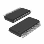 9DB801CFLF
The activity of extra discounts on wholesale prices is in full swing…
Please fill in your contact information and we will send you the latest wholesale price list.





