 ChipApex | Global Electronic Components Supplier
9DB801CGLF
Search Product
Search Post
— IC芯片 | 连接器 | 传感器 | 被动器件 —
Search productSearch post
— IC芯片 | 连接器 | 传感器 | 被动器件 —
Consult the customer manager about the wholesale price.
consultation hotline:86-132-6715-2157
email:[email protected]
Contact the product manager for consultation. One-stop consultation is available.
Do you want a lower wholesale price? Please send us your inquiry and we will reply immediately.
The Renesas 9DB801CGLF is a PCI Express (PCIe) zero-delay buffer integrated circuit designed for high-speed clock distribution. It features an input-to-output ratio of 1:8, supporting differential HCSL inputs and differential LVDS outputs. The device operates within a supply voltage range of 3.135V to 3.465V and supports maximum frequencies up to 400MHz. Packaged in a 48-TSSOP surface-mount format, it functions within an industrial temperature range of 0°C to 70°C. This component is engineered to maintain signal integrity in PCIe Gen1 applications by eliminating propagation delay skew between the single input and eight buffered outputs.
The 9DB801CGLF is listed as a discontinued product by Renesas Electronics Corporation. Verification of availability should focus on surplus distributors or existing stock rather than direct manufacturing orders. Buyers must confirm the specific suffix 'C' denotes the TSSOP-48 package variant and verify RoHS compliance status through current datasheets, as end-of-life notices may affect long-term sourcing reliability.
Select the 9DB801CGLF when designing PCIe Gen1 systems requiring a single source clock to drive eight downstream components with strict timing alignment. Ensure the design accommodates the 3.135V to 3.465V power rail requirements. Verify that the target PCB layout supports the 48-TSSOP footprint. For higher generation PCIe standards or different I/O voltage levels, alternative models such as the 9DB803 series should be evaluated.
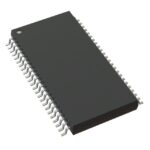 9DB801CGLF
The activity of extra discounts on wholesale prices is in full swing…
Please fill in your contact information and we will send you the latest wholesale price list.





