 ChipApex | Global Electronic Components Supplier
9DB803DGLFT
Search Product
Search Post
— IC芯片 | 连接器 | 传感器 | 被动器件 —
Search productSearch post
— IC芯片 | 连接器 | 传感器 | 被动器件 —
Consult the customer manager about the wholesale price.
consultation hotline:86-132-6715-2157
email:[email protected]
Contact the product manager for consultation. One-stop consultation is available.
Do you want a lower wholesale price? Please send us your inquiry and we will reply immediately.
The Renesas 9DB803DGLFT is an eight-output differential clock buffer designed for PCI Express Gen2 applications. It operates within a supply voltage range of 3.135 V to 3.465 V and supports maximum input frequencies up to 400 MHz. The device features zero propagation delay, cycle-cycle jitter under 50 ps, and PCIe Gen2 phase jitter below 3.0/3.1 ps rms. Packaged in a 48-pin SSOP with dimensions of 15.9 x 7.5 x 2.3 mm, it consumes typical power of 578 mW and functions as a zero-delay buffer or fanout driver.
Verify the suffix DGLF against the source material to confirm package type and temperature range. Confirm RoHS compliance status via official documentation before procurement. Check for moisture sensitivity level requirements during storage and handling.
Select this component when eight differential outputs are required for PCIe Gen2 systems. Ensure the design accommodates the 48-pin SSOP footprint. Verify that the input clock source matches the HCSL signaling specification and frequency range requirements.
This part belongs to the 9DB803 series of clock buffers from Renesas Electronics. It is compatible with the Intel DB800v2 Differential Buffer Specification and is typically driven by main clock generators such as the CK410B+, CK505, or CK509B.
The 9DB803DFLF is a verified alternative within the same family, differing primarily in operating temperature range (-40°C to +85°C versus 0°C to +70°C). Verify pin compatibility and electrical specifications before substitution.
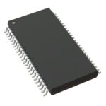 9DB803DGLFT
The activity of extra discounts on wholesale prices is in full swing…
Please fill in your contact information and we will send you the latest wholesale price list.






