 ChipApex | Global Electronic Components Supplier
9DB833AFILFT
Search Product
Search Post
— IC芯片 | 连接器 | 传感器 | 被动器件 —
Search productSearch post
— IC芯片 | 连接器 | 传感器 | 被动器件 —
Consult the customer manager about the wholesale price.
consultation hotline:86-132-6715-2157
email:[email protected]
Contact the product manager for consultation. One-stop consultation is available.
Do you want a lower wholesale price? Please send us your inquiry and we will reply immediately.
The Renesas 9DB833AFILFT is a PCIe Gen1/Gen2/Gen3 zero-delay buffer and fanout clock distribution IC. It features eight differential HCSL output pairs with phase jitter performance of less than 1ps RMS for PCIe Gen3, less than 3.1ps RMS for Gen2, and less than 86ps peak-to-peak for Gen1. The device operates at frequencies up to 166MHz in bypass mode and supports bandwidth programming from 50MHz to 110MHz in PLL mode. Powered by a single 3.3V supply (3.135V to 3.465V), it consumes approximately 528mW typical power. Packaged in a 48-pin TSSOP, it accepts spread spectrum input signals.
Verify component status as the 9DB833AFILFT may be listed as obsolete or not recommended for new designs in certain distributor databases. Confirm RoHS3 compliance and moisture sensitivity level (MSL 3) prior to procurement. Ensure the specific suffix matches the required package and tape/reel configuration for automated assembly processes.
Select this component when designing for PCIe Gen3 requirements while maintaining backward compatibility with Gen1 and Gen2 standards. Choose the 9DB833AFILFT over other family members if eight differential outputs are required. Verify that the system clock generator provides a compatible differential HCSL input signal, such as from a 932S421 or equivalent source.
The 9DB833AFILFT belongs to the 9DB833 series of clock buffers manufactured by Renesas Electronics. It is part of a broader portfolio of PCIe-compatible timing solutions designed to meet stringent jitter and skew requirements for modern high-speed serial interfaces. The device serves as a critical interface between main clock generators and multiple endpoint devices.
Publicly confirmed substitute part numbers include the 9DBL0841, 9DBL0851, and 9ZXL0853E. These alternatives offer similar 8-output configurations but may differ in specific package types, additional features like SMBus write protection, or exact electrical characteristics. Validate pinout and parameter compatibility before substitution.
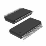 9DB833AFILFT
The activity of extra discounts on wholesale prices is in full swing…
Please fill in your contact information and we will send you the latest wholesale price list.





