 ChipApex | Global Electronic Components Supplier
9DB833AGLF
Search Product
Search Post
— IC芯片 | 连接器 | 传感器 | 被动器件 —
Search productSearch post
— IC芯片 | 连接器 | 传感器 | 被动器件 —
Consult the customer manager about the wholesale price.
consultation hotline:86-132-6715-2157
email:[email protected]
Contact the product manager for consultation. One-stop consultation is available.
Do you want a lower wholesale price? Please send us your inquiry and we will reply immediately.
The Renesas 9DB833AGLF is an eight-output PCIe Gen3 zero-delay buffer and fanout clock distribution IC. It operates within a supply voltage range of 3.135 V to 3.465 V and supports maximum input frequencies up to 166 MHz. The device features differential HCSL output signaling with a maximum propagation delay of 0 ps. Designed for surface-mount assembly, it is housed in a TSSOP-48 package. The component functions reliably across an operating temperature range from -40 °C to +85 °C, ensuring stable clock distribution for high-speed serial interfaces.
Verify the specific suffix 'GLF' against current manufacturer documentation to confirm RoHS compliance status and lead-free pin availability. Confirm that the TSSOP-48 package dimensions match the target PCB footprint design. Ensure the operating temperature grade (-40 °C to +85 °C) aligns with the environmental requirements of the final application system.
Select this component when eight differential clock outputs are required for PCIe Gen3 applications. The zero-delay buffer architecture minimizes skew between the input reference and output clocks. Verify that the driving source, such as the 932S421 or 932SQ420, provides compatible differential HCSL signaling. Ensure the power supply rails remain strictly within the 3.135 V to 3.465 V specification during operation.
This part belongs to the 9DB833 series of clock buffers designed specifically for PCI Express standards. It serves as a critical interface between main clock generators and peripheral devices requiring precise timing. The device replaces older generation buffers by supporting higher data rates while maintaining backward compatibility with legacy PCIe implementations.
The 9DB833AFLFT is listed as a discontinued alternative. Designers should verify if the 9DB833AGILFT serves as a direct functional replacement, noting potential differences in packaging or manufacturing site markings.
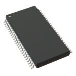 9DB833AGLF
The activity of extra discounts on wholesale prices is in full swing…
Please fill in your contact information and we will send you the latest wholesale price list.






