 ChipApex | Global Electronic Components Supplier
9DB833AGLFT
Search Product
Search Post
— IC芯片 | 连接器 | 传感器 | 被动器件 —
Search productSearch post
— IC芯片 | 连接器 | 传感器 | 被动器件 —
Consult the customer manager about the wholesale price.
consultation hotline:86-132-6715-2157
email:[email protected]
Contact the product manager for consultation. One-stop consultation is available.
Do you want a lower wholesale price? Please send us your inquiry and we will reply immediately.
The 9DB833AGLFT is a clock buffer manufactured by Renesas Electronics, designed for PCI Express Gen 3 applications. It features eight outputs and operates within a supply voltage range of 3.135 V to 3.465 V. The device supports a maximum input frequency of 166 MHz and maintains a maximum propagation delay of 0 ps. It is housed in a TSSOP-48 package and functions reliably across an operating temperature range from -40°C to +85°C.
Verify the specific suffix 'GLFT' against official Renesas documentation to confirm package type and tape-and-reel packaging details. Ensure compatibility with existing PCB footprints for the TSSOP-48 form factor. Cross-reference RoHS compliance status with current regulatory standards before procurement integration.
Select this component when eight buffered clock outputs are required for PCIe Gen 3 architectures. Confirm that the 3.135 V to 3.465 V supply voltage aligns with system power rails. Evaluate thermal management needs given the industrial temperature range and ensure the TSSOP-48 package fits the available board space constraints.
This part belongs to the 9DB833 series of zero-delay clock buffers. It serves as a signal conditioning component for high-speed serial interfaces. The device integrates PLL technology to maintain signal integrity across multiple loads. It is distinct from lower-output variants like the 9DB233 or 9DB433.
Publicly confirmed substitute part numbers for the 9DB833AGLFT were not identified in the provided source material. Verify pin-to-pin compatibility with any alternative components through official datasheet comparison.
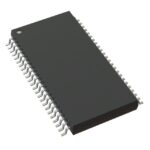 9DB833AGLFT
The activity of extra discounts on wholesale prices is in full swing…
Please fill in your contact information and we will send you the latest wholesale price list.





