 ChipApex | Global Electronic Components Supplier
9DBL0242BKILFT
Search Product
Search Post
— IC芯片 | 连接器 | 传感器 | 被动器件 —
Search productSearch post
— IC芯片 | 连接器 | 传感器 | 被动器件 —
Consult the customer manager about the wholesale price.
consultation hotline:86-132-6715-2157
email:[email protected]
Contact the product manager for consultation. One-stop consultation is available.
Do you want a lower wholesale price? Please send us your inquiry and we will reply immediately.
The 9DBL0242BKILFT is a 3.3V PCIe clock buffer manufactured by Renesas Electronics Corporation, designed for high-performance computing and networking applications. It features two differential outputs with Low Power HCSL (LP-HCSL) signaling, supporting frequencies from 1 MHz to 200 MHz. The device operates within a supply voltage range of 3.135 V to 3.465 V and includes integrated 100Ω termination resistors for direct connection to transmission lines. Packaged in a compact 4mm x 4mm 24-VFQFPN format, it supports spread spectrum clocking architectures including Common Clocked (CC), Separate Reference Independent Spread (SRIS), and Separate Reference No Spread (SRNS).
Verify the specific suffix 'BKI' against official Renesas documentation to confirm package type and tape/reel specifications. Ensure compatibility with system requirements for LP-HCSL signaling and 100Ω termination. Confirm operating temperature ranges align with application constraints before procurement.
Select this component when a low-pin-count solution is required for distributing PCIe reference clocks. The integrated 100Ω terminations simplify board layout compared to buffers requiring external resistors. Verify that the input frequency range of 1 MHz to 200 MHz matches the source clock generator capabilities.
This part belongs to the Renesas 9DBL0x series of fan-out buffers, which are optimized for PCIe clock distribution. These devices provide low-power HCSL outputs and support various PCIe clocking architectures. The series is designed to replace discrete resistor networks and standard buffers in high-speed digital designs.
Check for updated versions within the 9DBL0x family or alternative Renesas PCIe buffers with similar pin counts and termination configurations. Ensure any substitute maintains LP-HCSL output signaling and compatible supply voltage ranges.
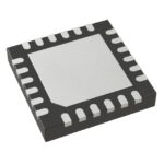 9DBL0242BKILFT
The activity of extra discounts on wholesale prices is in full swing…
Please fill in your contact information and we will send you the latest wholesale price list.





