 ChipApex | Global Electronic Components Supplier
9DBL0252BKILF/W
Search Product
Search Post
— IC芯片 | 连接器 | 传感器 | 被动器件 —
Search productSearch post
— IC芯片 | 连接器 | 传感器 | 被动器件 —
Consult the customer manager about the wholesale price.
consultation hotline:86-132-6715-2157
email:[email protected]
Contact the product manager for consultation. One-stop consultation is available.
Do you want a lower wholesale price? Please send us your inquiry and we will reply immediately.
The 9DBL0252BKILF/W is a 3.3V PCIe zero-delay buffer manufactured by Renesas Electronics Corporation. It features one differential HCSL input and two differential LP-HCSL outputs, supporting frequencies from 1 MHz to 200 MHz. The device operates within a supply voltage range of 3.135V to 3.465V and is housed in a 32-pin VFQFPN package measuring 5mm x 5mm. It supports PCIe Gen 1 through Gen 6 architectures.
Verify the specific suffix 'W' against official Renesas documentation to confirm if it denotes a specific tape-and-reel quantity or packaging variant distinct from standard listings. Confirm RoHS compliance status and current lifecycle stage, as this component family has undergone multiple production changes and end-of-life notices.
Select this component when a single-ended or differential source requires splitting into two matched zero-delay paths for PCIe applications. Ensure the design accommodates the 3.3V supply requirement and the 32-pin VFQFPN footprint constraints.
This part belongs to the 9DBL0x series of PCIe clock buffers. It serves as a fanout and jitter cleaning solution for high-speed serial interfaces. The manufacturer transitioned from Integrated Device Technology (IDT) to Renesas Electronics Corporation during product line acquisitions.
Officially recommended substitutes include other members of the 9DBL0x family, such as the 9DBL0452 or 9DBL0841, depending on the required output count.
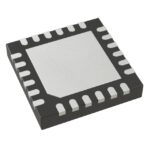 9DBL0252BKILF/W
The activity of extra discounts on wholesale prices is in full swing…
Please fill in your contact information and we will send you the latest wholesale price list.





