 ChipApex | Global Electronic Components Supplier
9DBL0252CKILFT
Search Product
Search Post
— IC芯片 | 连接器 | 传感器 | 被动器件 —
Search productSearch post
— IC芯片 | 连接器 | 传感器 | 被动器件 —
Consult the customer manager about the wholesale price.
consultation hotline:86-132-6715-2157
email:[email protected]
Contact the product manager for consultation. One-stop consultation is available.
Do you want a lower wholesale price? Please send us your inquiry and we will reply immediately.
The 9DBL0252CKILFT is a 2:4 clock mux buffer from Renesas Electronics, designed for PCIe Gen 1–7 applications. It operates at 3.3V and features four LP-HCSL differential outputs with integrated 100Ω terminations. The device supports Common Clocked (CC), Separate Reference Independent Spread (SRIS), and Separate Reference No Spread (SRNS) architectures. It accepts two HCSL inputs and provides selectable asynchronous or glitch-free switching modes. Packaged in a compact 32-VFQFPN format, it maximizes input frequency up to 125 MHz within a -40°C to +85°C operating range.
Verify the RoHS compliance status and Moisture Sensitivity Level (MSL) rating prior to procurement. Confirm that the 32-VFQFPN package dimensions align with the target PCB footprint. Ensure the supply voltage remains strictly within the 3.135 V to 3.465 V range to maintain signal integrity and operational stability.
Select this component when a single reference clock must be distributed to multiple PCIe endpoints using LP-HCSL signaling. The integrated 100Ω termination eliminates external resistor requirements, reducing board space. Choose the glitch-free switching mode if seamless transitions between input sources are required during operation without introducing timing errors.
This part belongs to the 9DBL0442 family of PCIe clock buffers. While the 9DBL0442 typically denotes a 4-output configuration, the 9DBL0252 variant specifically addresses 2-input to 4-output multiplexing needs. It shares the same 3.3V LP-HCSL output signaling and PCIe Gen 1–7 compatibility as its siblings in the series.
Direct substitutes include other 2:4 PCIe clock muxes from Renesas such as the 9DML04 series. Verify that replacement parts support the same LP-HCSL output type and integrated 100Ω termination to ensure pin-to-pin and functional compatibility.
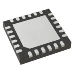 9DBL0252CKILFT
The activity of extra discounts on wholesale prices is in full swing…
Please fill in your contact information and we will send you the latest wholesale price list.







