 ChipApex | Global Electronic Components Supplier
9DBL0255NLGI8
Search Product
Search Post
— IC芯片 | 连接器 | 传感器 | 被动器件 —
Search productSearch post
— IC芯片 | 连接器 | 传感器 | 被动器件 —
Consult the customer manager about the wholesale price.
consultation hotline:86-132-6715-2157
email:[email protected]
Contact the product manager for consultation. One-stop consultation is available.
Do you want a lower wholesale price? Please send us your inquiry and we will reply immediately.
The 9DBL0255NLGI8 is a PCIe clock fanout buffer manufactured by Renesas Electronics Corporation. It operates at a maximum frequency of 220MHz and supports PCIe Gen1 through Gen7 standards. The device provides 2 or 4 outputs with a 1:2 input-to-output ratio, powered by a single 3.3V supply. It features a Loss of Signal (LOS) function for link integrity monitoring. The component is housed in a compact 16-VFQFPN package measuring 3x3 mm with an exposed pad, designed for surface-mount assembly.
Verify the specific suffix configuration against the official Renesas datasheet to ensure compatibility with required output counts and signal levels. Confirm that the 16-VFQFPN footprint matches the target PCB design constraints. Check current availability status as electronic components may experience supply fluctuations. Ensure compliance with RoHS3 regulations if required by project specifications.
Select this component when designing systems requiring robust clock distribution for PCIe interfaces up to Gen7 speeds. It is suitable for applications needing integrated loss-of-signal monitoring to maintain link stability. Consider the 3.3V operating voltage and the specific pinout requirements of the 16-VFQFPN package during schematic capture and layout phases.
This part belongs to the 9DBL series of clock buffers specialized for PCI Express applications. It complements other Renesas timing solutions by providing reliable fanout capabilities for high-speed serial links. The device addresses the need for low-jitter clock distribution in modern computing and communication hardware architectures.
Consult the Renesas product selection guide for direct substitutes within the 9DBL family. Verify pin-to-pin compatibility and electrical parameter equivalence before substitution.
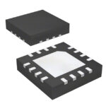 9DBL0255NLGI8
The activity of extra discounts on wholesale prices is in full swing…
Please fill in your contact information and we will send you the latest wholesale price list.





