 ChipApex | Global Electronic Components Supplier
9DBL0443ANLGI8
Search Product
Search Post
— IC芯片 | 连接器 | 传感器 | 被动器件 —
Search productSearch post
— IC芯片 | 连接器 | 传感器 | 被动器件 —
Consult the customer manager about the wholesale price.
consultation hotline:86-132-6715-2157
email:[email protected]
Contact the product manager for consultation. One-stop consultation is available.
Do you want a lower wholesale price? Please send us your inquiry and we will reply immediately.
The 9DBL0443ANLGI8 is a clock buffer from the Renesas 9DBL0x series, designed for PCIe Gen1 through Gen5 applications. It features four low-power HCSL (LP-HCSL) outputs with integrated 100Ω termination resistors, eliminating external components. The device operates in fanout mode at frequencies from 1MHz to 200MHz and supports Common Clock (CC) and Independent Reference (IR) architectures with spread spectrum tolerance. It includes three selectable SMBus addresses and dedicated output enable pins.
Verify the specific suffix 'NLGI8' against the official datasheet to confirm package type and tape-and-reel specifications. Ensure compatibility with required operating temperatures and voltage levels. Cross-reference the manufacturer part number with authorized distributors to avoid counterfeit components. Confirm RoHS compliance status as indicated in the product documentation.
Select this component when designing PCIe Gen1–Gen5 interfaces requiring integrated 100Ω termination. It is suitable for applications needing low power consumption and reduced bill of materials due to eliminated external resistors. Consider its support for spread spectrum clocking if EMI reduction is a priority. Verify that the 1MHz–200MHz frequency range meets system timing requirements.
This part belongs to the Renesas 9DBL0x family of low-power, high-performance clock buffers. These devices are optimized for PCIe clock distribution, offering multiple output configurations and flexible addressing. The family supports various termination options and packaging styles to accommodate different board space constraints and design needs.
Check for other members of the 9DBL0x family with compatible output counts and termination values. Verify pin-to-pin compatibility if substituting within the same series. Ensure alternative parts support the same PCIe generation standards and frequency ranges.
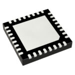 9DBL0443ANLGI8
The activity of extra discounts on wholesale prices is in full swing…
Please fill in your contact information and we will send you the latest wholesale price list.





