 ChipApex | Global Electronic Components Supplier
9DBL0452BKILF
Search Product
Search Post
— IC芯片 | 连接器 | 传感器 | 被动器件 —
Search productSearch post
— IC芯片 | 连接器 | 传感器 | 被动器件 —
Consult the customer manager about the wholesale price.
consultation hotline:86-132-6715-2157
email:[email protected]
Contact the product manager for consultation. One-stop consultation is available.
Do you want a lower wholesale price? Please send us your inquiry and we will reply immediately.
The 9DBL0452BKILF is a 4-output, 3.3V PCIe zero-delay/fanout clock buffer manufactured by Renesas Electronics. It supports PCIe Gen 1 through Gen 6 and accommodates both Common and Independent Reference Clock architectures. The device features four Low Power HCSL (LP-HSCl) outputs designed for direct connection to 85Ω transmission lines, eliminating the need for external series resistors. It operates with a supply voltage of 3.3V and accepts spread spectrum input signals. The component is housed in a space-saving 32-pin, 5mm × 5mm VFQFPN package.
Verify the specific suffix 'B' against official Renesas documentation to confirm pin-to-pin compatibility or functional differences compared to standard variants like the CKILF version. Confirm moisture sensitivity levels and reflow soldering profiles prior to assembly. Ensure the 32-pin VFQFPN footprint matches the design layout exactly.
Select this component when designing for PCIe Gen 6 applications requiring strict jitter specifications. Choose the ZDB mode for phase alignment requirements or Fanout mode for minimal jitter addition. Verify that the 3.3V supply voltage aligns with the system power rails and that the LP-HCSL output signaling is compatible with downstream receiver inputs.
The 9DBL0452 belongs to the 9DBL04 family of high-performance clock buffers. This product line has been acquired by SiTime, with full transition expected by the end of 2026. Documentation and ordering remain available via Renesas until that date, after which support shifts to SiTime.
Publicly confirmed substitute part numbers are not available in the provided source material. Consult SiTime or Renesas technical support for verified cross-references.
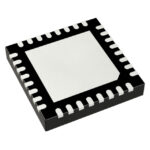 9DBL0452BKILF
The activity of extra discounts on wholesale prices is in full swing…
Please fill in your contact information and we will send you the latest wholesale price list.





