 ChipApex | Global Electronic Components Supplier
9DBL0453ANLGI
Search Product
Search Post
— IC芯片 | 连接器 | 传感器 | 被动器件 —
Search productSearch post
— IC芯片 | 连接器 | 传感器 | 被动器件 —
Consult the customer manager about the wholesale price.
consultation hotline:86-132-6715-2157
email:[email protected]
Contact the product manager for consultation. One-stop consultation is available.
Do you want a lower wholesale price? Please send us your inquiry and we will reply immediately.
The 9DBL0453ANLGI is a 4-output, 3.3V PCIe zero-delay/fanout clock buffer from Renesas Electronics. It supports PCIe Gen 1 through Gen 6 architectures, including Common Clock (CC) and Independent Reference (IR) modes with spread spectrum tolerance. The device features four Low Power HCSL (LP-HCSL) outputs that eliminate the need for external termination resistors per output pair. It offers additive phase jitter performance of less than 18fs RMS in fanout mode and less than 100fs RMS in high-bandwidth zero-delay buffer mode. Operating frequencies range from 1MHz to 200MHz. The component is housed in a space-saving 32-pin, 5mm x 5mm VFQFPN package.
Verify the specific suffix 'ANLGI' against official Renesas documentation to confirm exact tape-and-reel packaging specifications and moisture sensitivity level. Ensure compatibility with the target PCB footprint for the 32-VFQFPN package. Confirm that the required operating temperature range aligns with the standard industrial rating. Cross-reference the part number with the latest datasheet revision to ensure all electrical parameters match the design requirements.
Select this component when designing systems requiring low-jitter clock distribution for PCIe Gen 1 through Gen 6 interfaces. It is suitable for applications needing zero-delay buffering or fanout capabilities without external termination components. Consider this part for designs constrained by board space due to its compact 5mm x 5mm package. Verify that the input signal characteristics match the HCSL signaling requirements specified in the datasheet.
This device belongs to Renesas' comprehensive family of PCIe clock buffers and multiplexers. These components are engineered to meet the stringent timing and jitter requirements of modern PCI Express standards. The 9DBL series provides versatile solutions for clock generation and distribution in complex digital systems, ensuring signal integrity across various PCIe generations.
Yes, the device is tolerant of spread spectrum inputs, allowing for EMI reduction in the system design.
The device operates in fanout mode at frequencies ranging from 1MHz to 200MHz.
Each of the four outputs has a dedicated OE# pin, allowing for independent hardware control of each output channel.
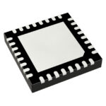 9DBL0453ANLGI
The activity of extra discounts on wholesale prices is in full swing…
Please fill in your contact information and we will send you the latest wholesale price list.





