 ChipApex | Global Electronic Components Supplier
9DBL0455NLGI8
Search Product
Search Post
— IC芯片 | 连接器 | 传感器 | 被动器件 —
Search productSearch post
— IC芯片 | 连接器 | 传感器 | 被动器件 —
Consult the customer manager about the wholesale price.
consultation hotline:86-132-6715-2157
email:[email protected]
Contact the product manager for consultation. One-stop consultation is available.
Do you want a lower wholesale price? Please send us your inquiry and we will reply immediately.
The 9DBL0455NLGI8 is a 4-output zero-delay/fanout clock buffer manufactured by Renesas Electronics Corporation. It operates at 3.3V and supports PCIe Gen 1 through Gen 6 standards, accommodating both Common and Independent Reference Clock architectures. The device features low power HCSL (LP-HCSL) outputs that allow direct connection to 85Ω transmission lines without external resistors. It includes dedicated output enable pins for each channel and supports spread spectrum input tolerance. Configuration is managed via an SMBus interface with three selectable addresses.
This component belongs to the 9DBL04 family of PCIe clock buffers. It shares the same 32-pin 5mm × 5mm VFQFPN package and core functionality as variants like the 9DBL0452, differing primarily in specific configuration settings or manufacturing lot attributes defined by the ordering suffix.
The 9DBL0452 is a functionally similar member of the same product family sharing the same package and electrical characteristics. Verify specific configuration requirements against the datasheet before substitution.
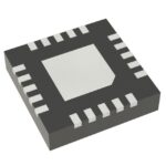 9DBL0455NLGI8
The activity of extra discounts on wholesale prices is in full swing…
Please fill in your contact information and we will send you the latest wholesale price list.






