ChipApex | Global Electronic Components Supplier
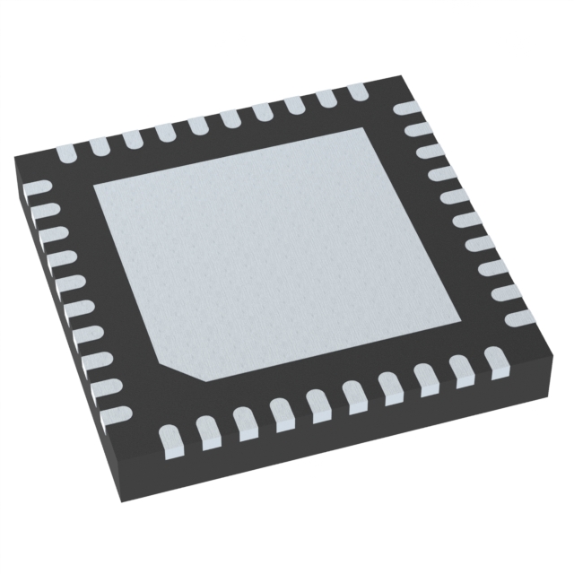
9DBL06P1B000KILF
Search Product
Search Post
— IC芯片 | 连接器 | 传感器 | 被动器件 —
Search productSearch post
— IC芯片 | 连接器 | 传感器 | 被动器件 —
Consult the customer manager about the wholesale price.
consultation hotline:86-132-6715-2157
email:[email protected]
Contact the product manager for consultation. One-stop consultation is available.
Do you want a lower wholesale price? Please send us your inquiry and we will reply immediately.
The 9DBL06P1B000KILF is a six-output, 3.3V PCIe zero-delay/fanout clock buffer manufactured by Renesas Electronics. It supports PCIe Gen 1 through Gen 6 architectures and accepts spread spectrum inputs. The device features low power HCSL (LP-HCSL) outputs that eliminate the need for external termination resistors per output pair. It allows direct connection to 85Ω transmission lines and includes dedicated OE# pins for each output. Configuration is managed via pin selection or SMBus interface with three selectable addresses.
Verify the specific suffix against official Renesas documentation to confirm package type and temperature range. Ensure compatibility with system voltage requirements of 3.3V. Confirm signal integrity specifications match the target PCIe generation. Check for RoHS compliance status if required by procurement policy. Validate lead-free status through manufacturer datasheets.
Select this component when six synchronized PCIe clock outputs are required for high-speed data transfer applications. It is suitable for designs needing zero-delay buffering with spread spectrum tolerance. Consider its LP-HCSL output capability for simplified PCB layout by removing external resistors. Evaluate its SMBus configurability for flexible system integration. Ensure the operating frequency range meets the specific PCIe generation needs.
This part belongs to Renesas' PCIe clock buffer family, designed for high-performance computing and storage environments. It complements other clock generators and buffers in the portfolio by providing fanout and zero-delay buffering capabilities. The device addresses the increasing complexity of PCIe topologies in modern servers and networking equipment.
Consult official Renesas substitution guides for verified alternatives. Generic equivalents may not support identical PCIe Gen 6 jitter specifications or LP-HCSL signaling. Verify pin-to-pin compatibility and electrical characteristics before replacement.
 9DBL06P1B000KILF
The activity of extra discounts on wholesale prices is in full swing…
Please fill in your contact information and we will send you the latest wholesale price list.