 ChipApex | Global Electronic Components Supplier
9DBL0741BKILFT
Search Product
Search Post
— IC芯片 | 连接器 | 传感器 | 被动器件 —
Search productSearch post
— IC芯片 | 连接器 | 传感器 | 被动器件 —
Consult the customer manager about the wholesale price.
consultation hotline:86-132-6715-2157
email:[email protected]
Contact the product manager for consultation. One-stop consultation is available.
Do you want a lower wholesale price? Please send us your inquiry and we will reply immediately.
The 9DBL0741BKILFT is a zero-delay fanout buffer manufactured by Renesas Electronics Corporation, designed for PCI Express (PCIe) clock distribution. It features a single HCSL differential input and eight LP-HCSL differential outputs, providing a 1:8 ratio. The device operates at frequencies up to 200 MHz with a supply voltage range of 3.135 V to 3.465 V. Packaged in a 48-VFQFPN (6x6 mm) surface-mount format, it supports an operating temperature range of -40°C to +85°C. This component integrates phase-locked loop (PLL) capabilities to minimize jitter while maintaining signal integrity across high-speed digital interfaces.
Verify component status as the 9DBL0741 series may be subject to discontinuation notices. Confirm availability through authorized distributors or check for active replacement part numbers such as those in the 9DBL0841 family if pin-compatible alternatives are required. Ensure RoHS3 compliance matches specific project requirements before finalizing procurement orders.
Select this component when designing systems requiring eight differential clock outputs driven by a single source with minimal skew. Verify that the PCB layout supports the 48-VFQFPN package dimensions. Ensure the power supply rails remain within the specified 3.135 V to 3.465 V range to maintain timing accuracy and output amplitude specifications defined in the datasheet.
This part belongs to the Renesas 9DBL series of PCIe clock buffers and generators. These devices are engineered to meet the stringent jitter and skew requirements of modern high-speed serial interfaces. The 9DBL0741 variant specifically addresses designs needing eight output channels, distinguishing it from lower-channel variants like the 9DBL0441 or higher-channel options within the same product family.
Check for official replacement part numbers provided by Renesas Electronics, such as the 9DBL0841 series, which may offer similar functionality or enhanced features. Verify pin compatibility and electrical specifications before substituting to ensure seamless integration into existing hardware designs without requiring schematic modifications.
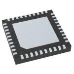 9DBL0741BKILFT
The activity of extra discounts on wholesale prices is in full swing…
Please fill in your contact information and we will send you the latest wholesale price list.





