 ChipApex | Global Electronic Components Supplier
9DBL0843ANDGI
Search Product
Search Post
— IC芯片 | 连接器 | 传感器 | 被动器件 —
Search productSearch post
— IC芯片 | 连接器 | 传感器 | 被动器件 —
Consult the customer manager about the wholesale price.
consultation hotline:86-132-6715-2157
email:[email protected]
Contact the product manager for consultation. One-stop consultation is available.
Do you want a lower wholesale price? Please send us your inquiry and we will reply immediately.
The 9DBL0843ANDGI is an eight-output, 3.3V PCIe zero-delay/fanout clock buffer manufactured by Renesas Electronics Corporation. It operates within a supply voltage range of 3.135V to 3.465V and delivers typical power consumption of 205mW. The device supports frequencies up to 200MHz with no programmable clock options and lacks reference output capabilities. Packaged in a 48-VFQFN exposed pad configuration, it provides robust signal distribution for high-speed data handling applications requiring precise timing performance.
Verify the specific package variant matches the 48-VFQFN Exposed Pad requirement. Confirm that the 3.3V supply specifications align with your target circuit design. Ensure compatibility with PCIe zero-delay buffering requirements before finalizing procurement decisions.
Select this component when eight distinct clock outputs are required from a single source. It is suitable for designs needing zero-delay buffering without programmable clock adjustments. Consider its 200MHz frequency limit and 205mW power consumption against system thermal constraints.
This part belongs to the 9DBL0843 series of clock buffers designed for high-speed digital interfaces. It serves as a critical timing element in complex electronic architectures where signal distribution fidelity is paramount. The device integrates advanced buffering technology to support modern high-bandwidth communication protocols.
Public confirmed substitute part numbers are not available in the provided documentation. Verify cross-reference data through official Renesas channels or authorized distributor databases before considering alternative components.
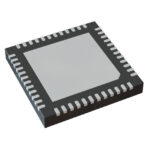 9DBL0843ANDGI
The activity of extra discounts on wholesale prices is in full swing…
Please fill in your contact information and we will send you the latest wholesale price list.







