 ChipApex | Global Electronic Components Supplier
9DBL0843ANDGI8
Search Product
Search Post
— IC芯片 | 连接器 | 传感器 | 被动器件 —
Search productSearch post
— IC芯片 | 连接器 | 传感器 | 被动器件 —
Consult the customer manager about the wholesale price.
consultation hotline:86-132-6715-2157
email:[email protected]
Contact the product manager for consultation. One-stop consultation is available.
Do you want a lower wholesale price? Please send us your inquiry and we will reply immediately.
The 9DBL0843ANDGI8 is a PCI Express zero-delay/fanout clock buffer manufactured by Renesas Electronics Corporation. It operates with a maximum frequency of 200MHz and features one input to eight outputs configuration. The device utilizes HCSL logic for both differential input and output signals. It is housed in a 48-VFQFPN (6x6) surface-mount package with exposed pad. The component supports a supply voltage range of 3.135V to 3.465V and functions within an industrial temperature range of -40°C to +85°C.
Verify the specific suffix 'GI8' against the official Renesas datasheet to confirm tape and reel packaging specifications and RoHS compliance status. Ensure the procurement source provides valid traceability documentation, as this component belongs to a specialized clock generation family requiring strict handling procedures during acquisition and storage.
Select this component when designing systems requiring precise phase alignment between reference and distributed clocks. The zero-delay architecture minimizes propagation delay variations. Engineers must ensure the load capacitance on each of the eight outputs remains within the datasheet limits to maintain signal integrity at the specified 200MHz operating frequency.
This part belongs to the 9DBL08x3 family of clock buffers designed specifically for PCI Express applications. It complements other variants like the 9DBL0841 series by offering different pinout or feature configurations while maintaining similar core timing performance characteristics for high-speed serial interface synchronization.
Public confirmed substitute part numbers are not available in the provided documentation. Verify compatibility with existing PCB layouts and power delivery networks before considering alternative components from the same manufacturer family.
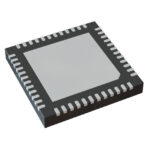 9DBL0843ANDGI8
The activity of extra discounts on wholesale prices is in full swing…
Please fill in your contact information and we will send you the latest wholesale price list.





