 ChipApex | Global Electronic Components Supplier
9DBU0241AKILFT
Search Product
Search Post
— IC芯片 | 连接器 | 传感器 | 被动器件 —
Search productSearch post
— IC芯片 | 连接器 | 传感器 | 被动器件 —
Consult the customer manager about the wholesale price.
consultation hotline:86-132-6715-2157
email:[email protected]
Contact the product manager for consultation. One-stop consultation is available.
Do you want a lower wholesale price? Please send us your inquiry and we will reply immediately.
The 9DBU0241AKILFT is a clock buffer manufactured by Renesas Electronics Corporation, designed for high-speed digital interfaces including PCI Express and Ethernet applications. It operates with a supply voltage range of 1.7V to 1.9V and features four low-power HCSL (LP-HCSL) outputs. The device supports input frequencies up to 137.5 MHz and functions within an industrial temperature range of -40°C to +85°C. Packaged in a compact 32-VFQFPN format with exposed pad, it integrates termination resistors for direct connection to transmission lines, reducing external component count.
Verify the suffix 'AKILFT' corresponds to the specific tape-and-reel packaging configuration and lead-free RoHS compliance status required for surface mount assembly. Confirm the moisture sensitivity level (MSL) rating prior to storage and reflow soldering processes to ensure component integrity during manufacturing.
Select this component when a four-channel fanout buffer with integrated terminations is required for 1.8V logic families. Ensure the input signal matches the supported HCSL or LVDS standards and that the operating frequency does not exceed 137.5 MHz. Compare power dissipation requirements against available thermal relief options on the PCB layout.
This part belongs to the 9DBU0241 family of ultra-low-power PCIe clock buffers. It serves as a zero-delay fanout solution for distributing reference clocks to multiple downstream components in high-speed serial link architectures, replacing discrete buffer circuits to save board space.
Direct replacements include the 9DBV0241AKILFT and 9DBU0241AKILF. Verify pin compatibility and electrical specifications before substitution, as package variations or voltage tolerances may differ between manufacturer suffixes.
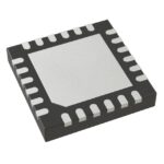 9DBU0241AKILFT
The activity of extra discounts on wholesale prices is in full swing…
Please fill in your contact information and we will send you the latest wholesale price list.






