 ChipApex | Global Electronic Components Supplier
9DBU0431AKLFT
Search Product
Search Post
— IC芯片 | 连接器 | 传感器 | 被动器件 —
Search productSearch post
— IC芯片 | 连接器 | 传感器 | 被动器件 —
Consult the customer manager about the wholesale price.
consultation hotline:86-132-6715-2157
email:[email protected]
Contact the product manager for consultation. One-stop consultation is available.
Do you want a lower wholesale price? Please send us your inquiry and we will reply immediately.
The 9DBU0431AKLFT is a PCIe zero-delay clock buffer manufactured by Renesas Electronics. It accepts an HCSL differential input and generates four LP-HCSL differential outputs, providing a 1:4 fan-out ratio. The device supports maximum frequencies up to 167 MHz and operates on a 1.5V supply voltage (1.425V to 1.575V). Packaged in a 32-VFQFPN with exposed pad, it functions within a temperature range of -40°C to 85°C.
Verify the package marking and date code against the manufacturer's latest datasheet to ensure authenticity. Confirm that the specific suffix matches the required tape-and-reel packaging format for automated assembly processes.
Select this component when a low-skew, zero-delay buffer is required for PCIe architectures. Ensure the design utilizes a 1.5V power rail and accommodates the 32-VFQFPN footprint. Verify thermal management requirements for the exposed pad under continuous operation at maximum frequency.
This part belongs to the 9DBU series of PCIe clock buffers. It complements other variants like the 9DBU0231 (2-output) and 9DBU0631 (6-output) to provide scalable clock distribution solutions for different lane counts in high-speed serial link applications.
Direct pin-to-pin replacements within the same family include the 9DBU0231AKILFT for reduced output count or the 9DBU0631AKILFT for increased fan-out. Verify electrical compatibility before substitution.
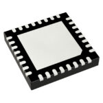 9DBU0431AKLFT
The activity of extra discounts on wholesale prices is in full swing…
Please fill in your contact information and we will send you the latest wholesale price list.






