 ChipApex | Global Electronic Components Supplier
9DBU0541AKILF
Search Product
Search Post
— IC芯片 | 连接器 | 传感器 | 被动器件 —
Search productSearch post
— IC芯片 | 连接器 | 传感器 | 被动器件 —
Consult the customer manager about the wholesale price.
consultation hotline:86-132-6715-2157
email:[email protected]
Contact the product manager for consultation. One-stop consultation is available.
Do you want a lower wholesale price? Please send us your inquiry and we will reply immediately.
The Renesas 9DBU0541AKILF is a PCI Express (PCIe) clock buffer IC designed for high-speed data transmission applications. It operates with a maximum frequency of 167MHz and provides one output channel. The device accepts HCSL differential input signals and generates LP-HCSL differential output signals, ensuring compatibility with PCIe Gen 1 through Gen 3 standards. It functions within a supply voltage range of 1.425V to 1.575V and supports an operating temperature range from -40°C to 85°C. The component is housed in a 32-VFQFPN package with dimensions of 5mm x 5mm, featuring exposed pads for thermal management and secure surface mount installation.
Verify the specific suffix 'AKILF' against the manufacturer's current datasheet to confirm pinout and electrical characteristics match the design requirements. Ensure that the 32-VFQFPN footprint on the PCB aligns precisely with the package dimensions provided in the official mechanical drawings. Confirm that the supply voltage rails can maintain stability within the 1.425V to 1.575V range under all load conditions.
Select this component when a single-channel PCIe clock buffer is required for Gen 1-3 applications. The HCSL-to-LP-HCSL conversion capability makes it suitable for driving low-power loads directly. Consider the 167MHz limit; if higher frequencies are needed, a different model from the 9DBU series or a higher-performance buffer must be chosen. The wide industrial temperature range (-40°C to 85°C) supports deployment in harsh environments.
This part belongs to the Renesas 9DBU family of PCIe clock buffers. These devices are engineered to provide clean, low-jitter clock signals for PCIe peripherals. The 9DBU0541 variant specifically offers a 1:1 ratio configuration, distinguishing it from fanout buffers with multiple outputs like the 9DBV series. It serves as a critical timing element in signal integrity chains for high-speed serial interfaces.
Direct replacements should be sought within the 9DBU series with matching I/O signaling (HCSL/LP-HCSL) and package type. Verify that any substitute maintains the same supply voltage constraints and frequency capabilities. Cross-referencing with the manufacturer's obsolescence notices is recommended to ensure long-term availability.
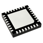 9DBU0541AKILF
The activity of extra discounts on wholesale prices is in full swing…
Please fill in your contact information and we will send you the latest wholesale price list.





