 ChipApex | Global Electronic Components Supplier
9DBU0631AKLF
Search Product
Search Post
— IC芯片 | 连接器 | 传感器 | 被动器件 —
Search productSearch post
— IC芯片 | 连接器 | 传感器 | 被动器件 —
Consult the customer manager about the wholesale price.
consultation hotline:86-132-6715-2157
email:[email protected]
Contact the product manager for consultation. One-stop consultation is available.
Do you want a lower wholesale price? Please send us your inquiry and we will reply immediately.
The Renesas 9DBU0631AKLF is a PCI Express zero-delay fanout buffer IC designed for clock distribution. It accepts an HCSL differential input and provides six LP-HCSL differential outputs with a 1:6 ratio. The device operates at a maximum frequency of 167 MHz within a supply voltage range of 1.425 V to 1.575 V. Packaged in a 40-VFQFPN (5x5 mm) surface-mount format, it supports industrial temperature ranges from -40°C to 85°C. This component integrates PLL functionality to attenuate jitter while maintaining low power consumption suitable for high-speed digital systems.
Verify the suffix 'LF' indicates lead-free compliance and standard tape-and-reel packaging. Confirm the specific temperature grade matches the application requirements, as commercial variants may differ from the industrial -40°C to 85°C rating found in related datasheets. Ensure the ordering part number aligns with the required package quantity and moisture sensitivity level specifications.
Select this component when a single source clock must drive multiple PCIe endpoints requiring LP-HCSL signaling. The 1:6 output ratio fits designs needing moderate fan-out without excessive board space. Verify that the input clock source meets HCSL voltage levels and that the system power budget accommodates the typical current draw associated with six active outputs at 167 MHz.
This part belongs to the 9DBU0631 family of ultra-low-power PCIe buffers. It shares architectural similarities with other members like the 9DBU0231 but offers higher output density. The device replaces older discrete buffering solutions by integrating PLL and termination functions into a compact 40-pin QFN package.
Direct pin-compatible substitutes within the same family include the 9DBU0631AKILFT, which differs primarily in packaging configuration. Cross-family replacements require verification of output count and voltage compatibility.
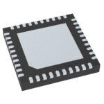 9DBU0631AKLF
The activity of extra discounts on wholesale prices is in full swing…
Please fill in your contact information and we will send you the latest wholesale price list.





