ChipApex | Global Electronic Components Supplier
9DBU0631AKLFT
Search Product
Search Post
— IC芯片 | 连接器 | 传感器 | 被动器件 —
Search productSearch post
— IC芯片 | 连接器 | 传感器 | 被动器件 —
Consult the customer manager about the wholesale price.
consultation hotline:86-132-6715-2157
email:[email protected]
Contact the product manager for consultation. One-stop consultation is available.
Do you want a lower wholesale price? Please send us your inquiry and we will reply immediately.
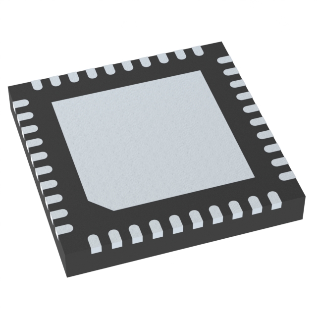
The Renesas 9DBU0631AKLFT is a PCI Express zero-delay buffer and fanout clock distribution IC. It accepts an HCSL differential input and provides six LP-HCSL differential outputs with a 1:6 ratio. The device operates at a maximum frequency of 167 MHz within a supply voltage range of 1.425 V to 1.575 V. Packaged in a 40-VFQFPN (5x5 mm) format, it supports an industrial temperature range from -40°C to 85°C. This component integrates PLL functionality for jitter attenuation while maintaining low power consumption suitable for high-speed digital systems.
Verify the suffix 'AKLFT' against official Renesas documentation to confirm package type, tape-and-reel packaging, and lead-free compliance status. Ensure the specific revision matches design requirements as manufacturing processes may update over time.
Select this model when a 1:6 fanout ratio with zero-delay buffering is required for PCIe interfaces. Compare against the 9DBU0231AKILFT if only two outputs are needed, or the 9DBU0441AKILFT for four outputs. Confirm that the LP-HCSL output swing meets the receiver specifications of the target devices.
This part belongs to the Renesas IDT 9DBU0631 family of ultra-low-power PCIe clock buffers. It serves as a direct replacement for legacy IDT parts with similar pinouts and electrical characteristics, facilitating migration in existing designs without significant layout changes.
The 9DBU0631AKLF is a tray-packaged variant of the same core device. Verify if the reel packaging of the AKLFT version is required for automated assembly processes compared to the manual loading of tray packages.
 9DBU0631AKLFT
The activity of extra discounts on wholesale prices is in full swing…
Please fill in your contact information and we will send you the latest wholesale price list.