 ChipApex | Global Electronic Components Supplier
9DBU0731AKILF
Search Product
Search Post
— IC芯片 | 连接器 | 传感器 | 被动器件 —
Search productSearch post
— IC芯片 | 连接器 | 传感器 | 被动器件 —
Consult the customer manager about the wholesale price.
consultation hotline:86-132-6715-2157
email:[email protected]
Contact the product manager for consultation. One-stop consultation is available.
Do you want a lower wholesale price? Please send us your inquiry and we will reply immediately.
The 9DBU0731AKILF is a PCIe fanout clock buffer manufactured by Renesas Electronics Corporation. It provides seven outputs from a single differential input, operating at a maximum frequency of 167MHz with a supply voltage range of 1.425V to 1.575V. The device features an additive phase jitter of typically 0.31ps RMS and supports PCIe Gen1, Gen2, and Gen3 standards. It is housed in a 40-MLF package and operates within a temperature range of -40°C to 85°C.
Verify the specific package variant and revision level against the official Renesas datasheet before procurement. Confirm that the application environment strictly adheres to the specified supply voltage and thermal operating ranges. Ensure compatibility with existing PCB layout constraints for the 40-MLF footprint to prevent integration issues during assembly.
Select this component when a single differential clock source must drive seven downstream loads with minimal signal degradation. It is suitable for designs requiring compliance with strict PCIe jitter masks across multiple generations. Consider the low power consumption profile and the availability of multiple SMBus addresses for flexible system management and monitoring capabilities.
This part belongs to the Renesas 9DBU series of PCIe clock buffers, designed specifically for high-performance computing applications. It complements other timing components like multiplexers and generators within the same ecosystem, ensuring coherent clock distribution across complex motherboard architectures while maintaining signal integrity standards.
No direct public substitute part numbers are confirmed for this discontinued component. Evaluate alternative PCIe clock buffers from Renesas or other manufacturers based on pin compatibility, electrical specifications, and package dimensions to ensure functional equivalence in existing designs.
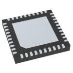 9DBU0731AKILF
The activity of extra discounts on wholesale prices is in full swing…
Please fill in your contact information and we will send you the latest wholesale price list.






