 ChipApex | Global Electronic Components Supplier
9DBV0231AKLFT
Search Product
Search Post
— IC芯片 | 连接器 | 传感器 | 被动器件 —
Search productSearch post
— IC芯片 | 连接器 | 传感器 | 被动器件 —
Consult the customer manager about the wholesale price.
consultation hotline:86-132-6715-2157
email:[email protected]
Contact the product manager for consultation. One-stop consultation is available.
Do you want a lower wholesale price? Please send us your inquiry and we will reply immediately.
The 9DBV0231AKLFT is a PCIe clock buffer and driver manufactured by Renesas Electronics. It operates with a single supply voltage ranging from 1.7V to 1.9V and supports maximum frequencies up to 137.5MHz. The device features one input and four differential outputs, utilizing HCSL signaling for both input and output interfaces. Packaged in a 32-VFQFN (5x5mm) surface-mount enclosure with an exposed pad, it is designed for low-power applications within an operating temperature range of -40°C to 85°C.
Verify the specific suffix 'AKLFT' against the manufacturer's current datasheet to confirm package type, lead finish, and tape-and-reel specifications. Ensure compatibility with the target PCB footprint for the 32-VFQFN package. Check for any recent Product Change Notifications (PCNs) that may affect material composition or manufacturing location.
Select this component when a zero-delay buffer with four differential outputs is required for PCIe designs. Compare input/output voltage levels and current drive capabilities against other loads on the bus. Consider thermal performance given the small 5x5mm package size and ensure adequate copper area for the exposed pad to maintain reliability within the specified temperature range.
This part belongs to the 9DBV series of ultra-low-power PCIe clock buffers. It serves as a fanout buffer to distribute a single reference clock to multiple endpoints while maintaining signal integrity. It is distinct from generators as it typically requires an external crystal or oscillator input rather than generating frequency from scratch without a reference.
Direct pin-to-pin replacements within the same family include the 9DBV0431AKILFT (4 outputs) or 9DBV0641AKLF (6 outputs) if additional channels are needed. Verify electrical parameters such as output swing and drive strength before substituting with non-Renesas equivalents.
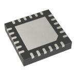 9DBV0231AKLFT
The activity of extra discounts on wholesale prices is in full swing…
Please fill in your contact information and we will send you the latest wholesale price list.





