 ChipApex | Global Electronic Components Supplier
9DBV0241AKLFT
Search Product
Search Post
— IC芯片 | 连接器 | 传感器 | 被动器件 —
Search productSearch post
— IC芯片 | 连接器 | 传感器 | 被动器件 —
Consult the customer manager about the wholesale price.
consultation hotline:86-132-6715-2157
email:[email protected]
Contact the product manager for consultation. One-stop consultation is available.
Do you want a lower wholesale price? Please send us your inquiry and we will reply immediately.
The 9DBV0241AKLFT is a 2-output, 1.8V PCIe Very-Low-Power (VLP) clock buffer from Renesas Electronics. It supports Zero-Delay and Fanout modes for PCI Express Gen1-3 applications. The device features LP-HCSL outputs with integrated 100Ω terminations, eliminating external resistors. Key specifications include a typical power consumption of 35mW in PLL mode, spread spectrum compatibility for EMI reduction, and SMBus-selectable features for signal integrity optimization. It operates within a standard temperature range and utilizes a space-saving 24-pin VFQFPN package.
Verify the specific suffix 'AKLFT' against the manufacturer's current datasheet to confirm pinout and packaging details. Ensure the design accounts for the 1.8V supply voltage requirement. Check for any recent Product Change Notifications (PCNs) regarding assembly sites or material changes, as Renesas has undergone organizational transitions affecting legacy IDT products.
Select this component when a 2-channel differential clock buffer with integrated 100Ω termination is required for PCIe interfaces. It is suitable for designs prioritizing low power consumption (35mW typical) and reduced bill-of-materials count due to eliminated external termination resistors. Verify that the input clock source is compatible with HCSL signaling standards.
This part belongs to the Renesas (formerly IDT) 1.8V Very-Low-Power PCIe family. It serves as a direct replacement for previous generation buffers by integrating termination resistors and offering SMBus configurability. The device is designed to meet the stringent power and signal integrity requirements of modern high-speed serial link architectures.
Direct replacements may include other members of the 9DBV series with different output counts, such as the 9DBV0541 (5-output) or 9DBV0941 (9-output), if additional channels are needed. Ensure pin compatibility when substituting with higher-output variants.
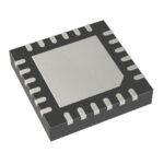 9DBV0241AKLFT
The activity of extra discounts on wholesale prices is in full swing…
Please fill in your contact information and we will send you the latest wholesale price list.





