 ChipApex | Global Electronic Components Supplier
9DBV0431AKLF
Search Product
Search Post
— IC芯片 | 连接器 | 传感器 | 被动器件 —
Search productSearch post
— IC芯片 | 连接器 | 传感器 | 被动器件 —
Consult the customer manager about the wholesale price.
consultation hotline:86-132-6715-2157
email:[email protected]
Contact the product manager for consultation. One-stop consultation is available.
Do you want a lower wholesale price? Please send us your inquiry and we will reply immediately.
The 9DBV0431AKLF is a PCIe clock buffer and driver manufactured by Renesas Electronics. It operates with a single HCSL input and provides four differential HCSL outputs, achieving a 1:4 fanout ratio. The device supports maximum frequencies up to 137.5 MHz and functions within a supply voltage range of 1.7 V to 1.9 V. Designed for Ethernet and PCI Express applications, it integrates termination resistors for direct connection to transmission lines. The component is housed in a 32-QFN (5x5 mm) package with an exposed pad, suitable for surface mount installation across an industrial temperature range of -40°C to 85°C.
Verify the specific suffix 'AKLF' against official Renesas documentation to confirm pinout compatibility and RoHS status. Confirm that the 32-QFN package dimensions match the target PCB footprint. Ensure the design accommodates the required 1.7 V to 1.9 V supply rail and thermal dissipation needs for the QFN package.
Select this component when a low-power, single-supply PCIe clock buffer is required. The 1:4 output configuration suits designs needing moderate fanout without complex PLL jitter cleaning. Verify that the HCSL input/output signaling levels align with the source clock generator and destination receiver specifications.
This part belongs to the 9DBVxx41 family of PCIe clock buffers. These devices are designed to replace legacy discrete clock distribution solutions. The 9DBV0431 variant specifically offers four outputs, distinguishing it from other members like the 9DBV0531 or 9DBV0731 which provide different fanout counts.
Direct replacements include other members of the 9DBV0431 series with compatible suffixes. Cross-family substitution requires verifying signal integrity and pin compatibility.
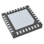 9DBV0431AKLF
The activity of extra discounts on wholesale prices is in full swing…
Please fill in your contact information and we will send you the latest wholesale price list.






