 ChipApex | Global Electronic Components Supplier
9DBV0441AKILFT
Search Product
Search Post
— IC芯片 | 连接器 | 传感器 | 被动器件 —
Search productSearch post
— IC芯片 | 连接器 | 传感器 | 被动器件 —
Consult the customer manager about the wholesale price.
consultation hotline:86-132-6715-2157
email:[email protected]
Contact the product manager for consultation. One-stop consultation is available.
Do you want a lower wholesale price? Please send us your inquiry and we will reply immediately.
The 9DBV0441AKILFT is a four-output, 1.8V PCIe zero-delay/fanout clock buffer manufactured by Renesas Electronics Corporation. It features integrated output terminations providing Zo = 100Ω for direct connection to transmission lines, eliminating external resistors. The device operates with LP-HCSL differential outputs and accepts HCSL differential inputs. It supports frequencies from 30 MHz to 137.5 MHz with typical power consumption of 65 mW in PLL mode. The component is housed in a space-saving 5x5 mm 32-VFQFPN package and includes programmable slew rate, output amplitude, and SMBus interface capabilities.
Verify the current lifecycle status as product availability may be subject to change. Confirm that the 32-VFQFPN package dimensions and pinout match the target PCB footprint. Ensure supply voltage requirements align with the 1.8V specification before integration into the design.
Select this component when a low-power, zero-delay fanout buffer with integrated termination is required for PCIe systems. It is suitable for designs needing programmable output characteristics to optimize signal integrity across varying trace lengths. Consider alternative models if higher operating frequencies or different supply voltages are necessary.
This part belongs to Renesas' SOC-friendly 1.8V Very-Low-Power (VLP) PCIe family. It is designed to minimize board space and power consumption while providing flexible clock management features. The device supports spread spectrum for EMI reduction and offers clean system start-up by blocking outputs until the PLL is locked.
The 9DBV0441BKLFT is listed as a manufacturer recomended substitute. Verify compatibility regarding package, electrical parameters, and functionality before substitution.
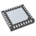 9DBV0441AKILFT
The activity of extra discounts on wholesale prices is in full swing…
Please fill in your contact information and we will send you the latest wholesale price list.





