ChipApex | Global Electronic Components Supplier
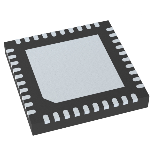
9DBV0631BKILFT
Search Product
Search Post
— IC芯片 | 连接器 | 传感器 | 被动器件 —
Search productSearch post
— IC芯片 | 连接器 | 传感器 | 被动器件 —
Consult the customer manager about the wholesale price.
consultation hotline:86-132-6715-2157
email:[email protected]
Contact the product manager for consultation. One-stop consultation is available.
Do you want a lower wholesale price? Please send us your inquiry and we will reply immediately.
The 9DBV0631BKILFT is a six-output, 1.8 V PCIe Gen1-2-3 Zero-Delay clock generator manufactured by Renesas Electronics. It supports differential input and output signaling with LP-HCSL output types. The device operates within a supply voltage range of 1.71 V to 1.89 V and features selectable SMBus addresses for configuration. It is designed for low-power applications in computing and networking systems requiring precise clock distribution.
Verify the complete part number including suffixes such as 'BKILFT' to ensure correct packaging and lead-free status. Confirm RoHS compliance details directly from the manufacturer's datasheet or authorized distributor documentation prior to procurement. Check for end-of-life notifications as availability may be limited.
Select this component when designing systems requiring six synchronized clock outputs with minimal skew for PCIe interfaces. Ensure the design accommodates the 1.8 V supply requirement and provides adequate filtering for the analog power rail. Consider thermal management and PCB layout constraints associated with high-speed differential signaling.
This device belongs to Renesas' family of ultra-low-power PCIe clock generators. It replaces older 3.3 V solutions, offering significant power reduction and board space savings. The zero-delay architecture ensures that output clocks are phase-aligned with the input reference, critical for high-speed data transmission integrity.
Direct substitutes include other Renesas 9DBV series devices with compatible pinouts and electrical characteristics. Verify compatibility with existing firmware and SMBus configurations before swapping components. Cross-reference with official replacement guides for discontinued variants.
 9DBV0631BKILFT
The activity of extra discounts on wholesale prices is in full swing…
Please fill in your contact information and we will send you the latest wholesale price list.