 ChipApex | Global Electronic Components Supplier
9DBV0641AKILF
Search Product
Search Post
— IC芯片 | 连接器 | 传感器 | 被动器件 —
Search productSearch post
— IC芯片 | 连接器 | 传感器 | 被动器件 —
Consult the customer manager about the wholesale price.
consultation hotline:86-132-6715-2157
email:[email protected]
Contact the product manager for consultation. One-stop consultation is available.
Do you want a lower wholesale price? Please send us your inquiry and we will reply immediately.
The Renesas 9DBV0641AKILF is a six-output, 1.8V PCIe Gen1/Gen2/Gen3 zero-delay clock generator. It supports input frequencies up to 200 MHz and provides LP-HCSL outputs with integrated 100Ω terminations for direct connection to transmission lines. The device features three selectable SMBus addresses and individual output enable pins for power management. Operating within a -40°C to +85°C temperature range, it utilizes a 40-pin VFQFPN package (5.0 x 5.0 x 0.9 mm) with 0.4 mm pitch.
Verify the specific suffix 'AKILF' against the official datasheet to confirm package type and operating temperature range. Confirm RoHS compliance status and moisture sensitivity level (MSL) requirements prior to assembly planning. Check for recent product change notifications regarding manufacturing site or material updates.
Select this component when a low-power, 1.8V zero-delay clock solution is required for PCIe applications. Ensure the design accommodates the 40-pin VFQFPN footprint. Verify that the system requires exactly six differential outputs and compatible LP-HCSL signaling levels.
This part belongs to the 9DBV0641 family of PCIe clock generators. It is designed to replace legacy clocking solutions in high-speed digital interfaces requiring precise timing alignment and low jitter performance for compliant signal integrity.
Consult the manufacturer's cross-reference guide for verified substitutes. Generic fanout buffers may lack the zero-delay PLL functionality or integrated termination resistors required for direct PCIe compliance.
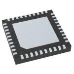 9DBV0641AKILF
The activity of extra discounts on wholesale prices is in full swing…
Please fill in your contact information and we will send you the latest wholesale price list.






