ChipApex | Global Electronic Components Supplier
9DBV0731AKLF
Search Product
Search Post
— IC芯片 | 连接器 | 传感器 | 被动器件 —
Search productSearch post
— IC芯片 | 连接器 | 传感器 | 被动器件 —
Consult the customer manager about the wholesale price.
consultation hotline:86-132-6715-2157
email:[email protected]
Contact the product manager for consultation. One-stop consultation is available.
Do you want a lower wholesale price? Please send us your inquiry and we will reply immediately.
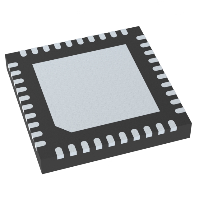
The 9DBV0731AKLF is a seven-output fanout clock buffer manufactured by Renesas Electronics, designed for PCI Express applications. It operates with a single 1.8V supply voltage and accepts HCSL differential inputs to generate LP-HCSL differential outputs. The device supports operating frequencies from 1 MHz to 200 MHz and features integrated 100-ohm terminations for direct connection to transmission lines. Key specifications include a typical power consumption of 50 mW, selectable SMBus addresses for configuration, and individual output enable pins for power management. It is housed in a space-saving 48-pin VFQFPN package.
Verify the specific suffix 'AKLF' against the manufacturer's current datasheet to confirm pinout compatibility and RoHS status. Check for Product Change Notifications (PCNs) regarding assembly site or material updates. Confirm moisture sensitivity level (MSL 3) handling requirements during storage and soldering processes.
Select this component when a seven-channel fanout buffer is required for 1.8V PCIe designs. Compare against the 9DBV0541 (5-output) and 9DBV0941 (9-output) variants if channel count differs. Ensure the host controller supports the SMBus configuration protocol if dynamic tuning of slew rates or amplitudes is needed.
This part belongs to the 9DBV05x1-07x1-09x1 family of PCIe fanout clock buffers. These devices are engineered to replace discrete resistor networks, saving board space and reducing component count. They are commonly used alongside PCIe clock generators like the 9FGV series to distribute reference clocks across multiple slots or peripherals.
Direct functional substitutes within the same family include the 9DBV0541 (5 outputs) and 9DBV0941 (9 outputs). Verify that the pinout remains compatible if substituting between different output counts in the same package.
 9DBV0731AKLF
The activity of extra discounts on wholesale prices is in full swing…
Please fill in your contact information and we will send you the latest wholesale price list.