 ChipApex | Global Electronic Components Supplier
9DBV0841AKILF
Search Product
Search Post
— IC芯片 | 连接器 | 传感器 | 被动器件 —
Search productSearch post
— IC芯片 | 连接器 | 传感器 | 被动器件 —
Consult the customer manager about the wholesale price.
consultation hotline:86-132-6715-2157
email:[email protected]
Contact the product manager for consultation. One-stop consultation is available.
Do you want a lower wholesale price? Please send us your inquiry and we will reply immediately.
The 9DBV0841AKILF is a clock buffer manufactured by Renesas Electronics Corporation, designed for PCI Express applications. It features one differential input and eight differential outputs with an input-to-output ratio of 1:8. The device operates at a maximum frequency of 200 MHz and supports HCSL signaling standards for both input and output. It utilizes a 48-VFQFN package with dimensions of 6x6 mm. The component functions as a zero-delay or fanout buffer within the PCIe clock distribution network.
Verify the specific suffix 'AKILF' against the manufacturer's current datasheet to confirm pinout compatibility and RoHS status. Check for Product Change Notifications (PCNs) regarding assembly site changes or package revisions. Confirm availability through authorized distributors as lead times may vary based on production cycles.
Select this component when eight low-power LVPECL/HCSL compatible outputs are required from a single HCSL source. Ensure the design accommodates the 3.3V supply voltage typical for this family member. Verify that the 48-VFQFN footprint matches the PCB layout constraints and thermal requirements for the target application environment.
This part belongs to the 9DBV05x1-07x1-09x1 family of PCIe fanout clock buffers. It shares architectural similarities with other members like the 9DBV0541 and 9DBV0941, differing primarily in the number of outputs. The family is characterized by integrated terminations and SMBus configurability for flexible system integration.
Direct substitutes within the same family include the 9DBV0541 (5 outputs) or 9DBV0941 (9 outputs), provided the output count difference is acceptable. Cross-family replacements such as the 9DBL series should be evaluated for voltage level compatibility and pinout alignment.
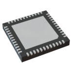 9DBV0841AKILF
The activity of extra discounts on wholesale prices is in full swing…
Please fill in your contact information and we will send you the latest wholesale price list.






