 ChipApex | Global Electronic Components Supplier
9DMU0431AKILFT
Search Product
Search Post
— IC芯片 | 连接器 | 传感器 | 被动器件 —
Search productSearch post
— IC芯片 | 连接器 | 传感器 | 被动器件 —
Consult the customer manager about the wholesale price.
consultation hotline:86-132-6715-2157
email:[email protected]
Contact the product manager for consultation. One-stop consultation is available.
Do you want a lower wholesale price? Please send us your inquiry and we will reply immediately.
The 9DMU0431AKILFT is a clock multiplexer IC designed for PCI Express (PCIe) Gen1, Gen2, and Gen3 applications. It operates with a supply voltage range of 1.425V to 1.575V and supports input frequencies up to 200MHz. The device features a 2:1 input-to-output ratio with differential inputs and outputs. It is housed in a 24-VFQFPN package with dimensions of 4.00x4.00x0.90 mm and an exposed pad. The component is RoHS compliant and intended for high-speed timing distribution.
Verify the specific ordering suffix and package variant against the official Renesas datasheet to ensure compatibility with design requirements. Confirm that the 1.425V to 1.575V supply voltage range aligns with the target system's power architecture. Ensure the 24-VFQFPN footprint matches the PCB layout specifications before finalizing procurement orders.
Select this component when designing for PCIe Gen1 through Gen3 interfaces requiring low-power clock distribution. The device offers a direct replacement path for legacy 3.3V HCSL solutions, reducing overall system power and physical footprint. Consider the 200MHz maximum frequency capability and the 2:1 multiplexing ratio when evaluating timing network complexity and signal routing constraints.
This part belongs to the 9DMU/V series of clock multiplexers from Renesas Electronics. The series is specifically engineered to address the power and size constraints of modern high-speed serial interfaces like PCIe. It complements other timing solutions such as buffers and generators within the same product family, providing specialized multiplexing functionality for complex clock trees.
Public confirmed substitute part numbers are not available in the provided documentation.
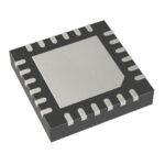 9DMU0431AKILFT
The activity of extra discounts on wholesale prices is in full swing…
Please fill in your contact information and we will send you the latest wholesale price list.





