 ChipApex | Global Electronic Components Supplier
9DMU0441AKILFT
Search Product
Search Post
— IC芯片 | 连接器 | 传感器 | 被动器件 —
Search productSearch post
— IC芯片 | 连接器 | 传感器 | 被动器件 —
Consult the customer manager about the wholesale price.
consultation hotline:86-132-6715-2157
email:[email protected]
Contact the product manager for consultation. One-stop consultation is available.
Do you want a lower wholesale price? Please send us your inquiry and we will reply immediately.
The 9DMU0441AKILFT is a 2:4 clock multiplexer from the Renesas IDT PCIe Gen1-2-3 family. It operates at 1.8V with LP-HCSL outputs featuring integrated 100-ohm terminations for direct transmission line connection. The device supports asynchronous or glitch-free switching, spread spectrum compatibility for EMI reduction, and individual output enables for power management. Operating frequency ranges from 1 MHz to 200 MHz within a 4x4 mm 24-pin VFQFPN package.
Verify the specific suffix against official Renesas documentation to confirm package type and temperature range. Ensure the ordering code matches the required switching mode configuration. Cross-reference the manufacturer part number with authorized distributors to avoid counterfeit components. Confirm lead times directly with the supplier as production cycles may vary.
Select this component when a 2-input to 4-output clock mux is required for PCIe applications. The integrated termination simplifies PCB layout compared to standard HCSL devices. Choose between asynchronous and glitch-free modes based on system startup requirements. Verify that the 1.8V supply voltage aligns with the target platform's power rails.
This device belongs to the IDT PCIe clock multiplexer family designed for system-on-chip integration. It replaces discrete resistor networks by providing on-chip termination. The series targets high-performance computing environments where board space and power consumption are critical constraints for clock distribution networks.
Consult official substitution guides for equivalent parts within the IDT portfolio. Verify pinout compatibility before replacing existing designs. Ensure the replacement supports the same PCIe generation standards and operating voltage levels.
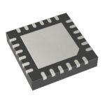 9DMU0441AKILFT
The activity of extra discounts on wholesale prices is in full swing…
Please fill in your contact information and we will send you the latest wholesale price list.





