 ChipApex | Global Electronic Components Supplier
9FGL0651CKILF
Search Product
Search Post
— IC芯片 | 连接器 | 传感器 | 被动器件 —
Search productSearch post
— IC芯片 | 连接器 | 传感器 | 被动器件 —
Consult the customer manager about the wholesale price.
consultation hotline:86-132-6715-2157
email:[email protected]
Contact the product manager for consultation. One-stop consultation is available.
Do you want a lower wholesale price? Please send us your inquiry and we will reply immediately.
The Renesas 9FGL0651CKILF is a PCIe clock generator IC designed for high-speed serial link applications. It operates with a single 3.3V supply and features six differential outputs utilizing LP-HCSL signaling. The device supports input frequencies of 25 MHz or 100 MHz, generating corresponding output clocks compliant with PCIe Gen 1 through Gen 6 standards. It incorporates an internal PLL for jitter attenuation and supports Common Clocked (CC), Separate Reference No Spread (SRNS), and Separate Reference Independent Spread (SRIS) architectures. The component is housed in a compact 24-VFQFPN package measuring 4mm x 4mm.
Verify the specific suffix 'CKILF' against official Renesas documentation to confirm package type and tape/reel specifications. Confirm current lifecycle status as distribution data indicates potential end-of-life notifications for this family. Ensure compatibility with required moisture sensitivity levels for surface mount assembly processes.
Select this model when six synchronized differential clock outputs are required for PCIe expansion slots or connectors. Verify that the system design utilizes a 3.3V power domain. Consider the 24-VFQFPN footprint constraints during PCB layout. Ensure the application requires LP-HCSL signaling rather than LVPECL or LVDS variants found in other Renesas clock buffers.
This component belongs to the 9FGL02x1/04x1/06x1/08x1 series of 3.3V PCIe clock generators. The part number structure indicates six outputs ('06') and a 25MHz base frequency option ('51'). It serves as a timing source for multi-lane PCIe interfaces, replacing discrete oscillator solutions to save board space and reduce jitter.
The 9FGL0251CKILFT provides two outputs in the same package. The 9FGL0451CKILFT offers four outputs. For eight outputs, the 9FGL0851CKILFT is the direct family member. Verify pinout compatibility if substituting between different output counts within this series.
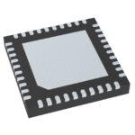 9FGL0651CKILF
The activity of extra discounts on wholesale prices is in full swing…
Please fill in your contact information and we will send you the latest wholesale price list.






