 ChipApex | Global Electronic Components Supplier
9FGL0851DKILFT
Search Product
Search Post
— IC芯片 | 连接器 | 传感器 | 被动器件 —
Search productSearch post
— IC芯片 | 连接器 | 传感器 | 被动器件 —
Consult the customer manager about the wholesale price.
consultation hotline:86-132-6715-2157
email:[email protected]
Contact the product manager for consultation. One-stop consultation is available.
Do you want a lower wholesale price? Please send us your inquiry and we will reply immediately.
The Renesas Electronics 9FGL0851DKILFT is an 8-output 3.3V PCIe Gen1-5 clock generator housed in a 48-VFQFPN package. It provides eight differential LP-HCSL outputs at 100MHz, each with a dedicated OE# pin for PCIe CLKREQ# functionality. The device supports Common Clocked (CC) and Independent Reference (IR) architectures including SRIS and SRNS. Key electrical specifications include a supply voltage range of 3.135V to 3.465V, typical power consumption of 112–206 mW, and 90fs RMS jitter compliance for PCIe Gen5 CC. Integrated terminations are available for both 100Ω and 85Ω systems.
Verify the specific suffix 'KILFT' against the manufacturer's official ordering guide to confirm packaging details such as reel size and tape width. Confirm RoHS compliance status directly from the datasheet documentation. Ensure the 48-VFQFPN package dimensions match the PCB footprint requirements before finalizing procurement.
Select this component when designing for PCIe Gen1 through Gen5 interfaces requiring up to eight differential clock outputs. Verify that the system requires either 100Ω or 85Ω integrated termination to utilize the space-saving feature. Ensure the design accommodates the 48-pin VFQFPN package and operates within the specified -40°C to +85°C temperature range.
This part belongs to the 9FGL02x1/04x1/06x1/08x1D family of 3.3V PCIe clock generators. While other members of the family offer 2, 4, or 6 outputs, the 9FGL0851DKILFT specifically provides eight differential outputs. It shares common features like PLL-based synthesis and SMBus configurability with its siblings but utilizes a larger 6mm x 6mm package to accommodate the additional pins.
Direct replacements within the same family include the 9FGL0651DKILFT (6 outputs) if fewer lanes are required. For applications needing fewer outputs, the 9FGL0451DKILFT or 9FGL0251DKILFT may be suitable. Ensure any substitute maintains the 48-VFQFPN form factor or verify pin compatibility if using a different package size.
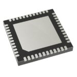 9FGL0851DKILFT
The activity of extra discounts on wholesale prices is in full swing…
Please fill in your contact information and we will send you the latest wholesale price list.






