 ChipApex | Global Electronic Components Supplier
9FGL6241AP302NDGI8
Search Product
Search Post
— IC芯片 | 连接器 | 传感器 | 被动器件 —
Search productSearch post
— IC芯片 | 连接器 | 传感器 | 被动器件 —
Consult the customer manager about the wholesale price.
consultation hotline:86-132-6715-2157
email:[email protected]
Contact the product manager for consultation. One-stop consultation is available.
Do you want a lower wholesale price? Please send us your inquiry and we will reply immediately.
The Renesas 9FGL6241AP302NDGI8 is a PCI Express (PCIe) clock generator IC designed for high-speed data transmission applications. It operates with a maximum frequency of 100MHz and provides one output channel. The device supports LP-HCSL and LVCMOS output signaling types, featuring a 3:2 input-to-output ratio. It utilizes a 28-VFQFPN (4x4mm) package with an exposed pad for surface mount installation. Power supply requirements include 1.71V to 1.89V, 2.375V to 3.465V, and 3.135V rails. The component functions within a temperature range of -40°C to 85°C.
Verify the specific suffix NDGI8 against official Renesas documentation to confirm tape and reel packaging specifications. Ensure compatibility with required voltage domains and thermal management strategies for the VFQFPN package. Confirm RoHS compliance status through current datasheets before procurement.
Select this model when a single differential output with 100Ω termination is required for PCIe Gen 1-6 interfaces. Compare with the 9FGL6251 series if two outputs or 85Ω termination options are needed. Verify that the 28-VFQFPN footprint aligns with PCB layout constraints.
This component belongs to the 9FGL6241/6251 family of intelligent PCIe clock buffers and generators. These devices are engineered to support various PCIe clocking architectures, providing flexibility for system designers implementing high-speed serial links in storage and computing platforms.
The 9FGL6251AP302NDGI8 serves as a functional alternative offering dual outputs instead of single. Designers requiring identical single-output performance should verify pinout compatibility and electrical parameters against the original specification.
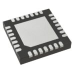 9FGL6241AP302NDGI8
The activity of extra discounts on wholesale prices is in full swing…
Please fill in your contact information and we will send you the latest wholesale price list.






