 ChipApex | Global Electronic Components Supplier
9FGL6251AP201NDGI
Search Product
Search Post
— IC芯片 | 连接器 | 传感器 | 被动器件 —
Search productSearch post
— IC芯片 | 连接器 | 传感器 | 被动器件 —
Consult the customer manager about the wholesale price.
consultation hotline:86-132-6715-2157
email:[email protected]
Contact the product manager for consultation. One-stop consultation is available.
Do you want a lower wholesale price? Please send us your inquiry and we will reply immediately.
The 9FGL6251AP201NDGI is a clock generator and buffer from the Renesas 9FGL6251 series, designed for PCIe and NVMe applications. It supports Common (CC) and Independent Reference (IR) architectures with automatic input clock detection and mode switching. The device features two differential LP-HCSL outputs with integrated 85Ω terminations, eliminating external resistors. It accepts 25MHz or 33.33MHz reference inputs via crystal or LVCMOS/LVDS signals. Operating voltage ranges from 2.5V to 3.3V, with a 1.8V supply for the reference input. The component is housed in a 28-VQFP-N package.
Verify the specific suffix 'P201' against official Renesas documentation to confirm pinout and electrical characteristics, as variations exist within the 9FGL6251 family. Confirm moisture sensitivity level and reel packaging quantities directly with the manufacturer or authorized distributors, as these parameters are critical for surface-mount assembly processes.
Select this component for designs requiring intelligent clock management in NVMe or PCIe environments. Ensure the design supports the required 2.5V or 3.3V VDD supply and 1.8V VDDREF. Verify that the integrated 85Ω output impedance matches the PCB trace requirements, distinguishing it from the 100Ω variant found in the 9FGL6241 series.
This part belongs to the 9FGL6251 series, which serves as the root platform for various configurations including 31, 41, and 51 suffixes. The series is optimized for high-performance storage controllers, providing flexible clock generation and distribution capabilities while reducing bill-of-materials count through integrated terminations and crystal options.
The 9FGL6251AQ302LTGI8 is a documented related part within the same series. Verify functional compatibility regarding output impedance and package type before substitution. Other members of the 9FGL6251 family may offer different pinouts or feature sets.
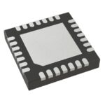 9FGL6251AP201NDGI
The activity of extra discounts on wholesale prices is in full swing…
Please fill in your contact information and we will send you the latest wholesale price list.





