 ChipApex | Global Electronic Components Supplier
9FGL6251AP202NDGI8
Search Product
Search Post
— IC芯片 | 连接器 | 传感器 | 被动器件 —
Search productSearch post
— IC芯片 | 连接器 | 传感器 | 被动器件 —
Consult the customer manager about the wholesale price.
consultation hotline:86-132-6715-2157
email:[email protected]
Contact the product manager for consultation. One-stop consultation is available.
Do you want a lower wholesale price? Please send us your inquiry and we will reply immediately.
The 9FGL6251AP202NDGI8 is a clock generator and buffer from the Renesas 9FGL6251 series, designed for PCIe Gen 1–6 applications. It features two differential LP-HCSL outputs with integrated 85Ω terminations. The device supports Common Clocked (CC) and Separate Reference Independent Spread (SRIS) architectures, defaulting to -0.5% spread spectrum. It accepts 25MHz or 33.33MHz reference inputs and operates on a 3.3V supply. The component is housed in a 4mm × 4mm 28-VQFP-N package.
Verify the specific suffix NDGI8 against the manufacturer's current datasheet to confirm packaging details and RoHS compliance status. Factory packaging quantity is listed as 2500 units per reel. Confirm moisture sensitivity level requirements during handling and storage prior to assembly.
Select this part for designs requiring integrated 85Ω termination to reduce external resistor count. Ensure the system architecture aligns with CC or SRIS modes, as the device defaults to -0.5% spread spectrum. Verify that the 25MHz or 33.33MHz reference frequency matches the host controller specifications.
This component belongs to the 9FGL6251 family, which includes variants like the 9FGL6241 and 9FGL6251AQ302LTGI8. The AP202 suffix indicates specific pinning and configuration options within the intelligent PCIe clock buffer line tailored for high-speed serial interface timing.
The 9FGL6241AP202NDGI8 is a related single-output variant within the same series. Cross-referencing the 9FGL6251AQ302LTGI8 may be necessary if internal crystal options or different spread spectrum configurations are required.
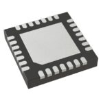 9FGL6251AP202NDGI8
The activity of extra discounts on wholesale prices is in full swing…
Please fill in your contact information and we will send you the latest wholesale price list.






