 ChipApex | Global Electronic Components Supplier
9FGL6251AP301NDGI8
Search Product
Search Post
— IC芯片 | 连接器 | 传感器 | 被动器件 —
Search productSearch post
— IC芯片 | 连接器 | 传感器 | 被动器件 —
Consult the customer manager about the wholesale price.
consultation hotline:86-132-6715-2157
email:[email protected]
Contact the product manager for consultation. One-stop consultation is available.
Do you want a lower wholesale price? Please send us your inquiry and we will reply immediately.
The 9FGL6251AP301NDGI8 is a clock generator and buffer from the Renesas 9FGL6251 series, designed for intelligent PCIe clock applications. It supports Common (CC) and Independent Reference (IR) architectures, featuring two differential LP-HCSL outputs with integrated 85Ω terminations. The device automatically detects input clocks and switches modes, offering SMBus-selectable spread spectrum clocking (-0.25% or -0.5%). It operates on 2.5V or 3.3V supplies, accepts 25MHz or 33.33MHz reference inputs, and is housed in a 4mm x 4mm 28-VQFP-N package.
Verify the specific suffix NDGI8 against official Renesas documentation to confirm reel packaging and lead-free status. Confirm that the AP301 variant matches the required spread spectrum configuration (-0.5%) for the target design. Ensure compatibility with the 28-VQFP-N package footprint during PCB layout.
Select this component when an intelligent buffer with automatic mode switching is required for NVMe or PCIe interfaces. The integrated output terminations reduce external BOM count. Verify that the 85Ω output impedance aligns with the downstream logic requirements, as other variants may offer 100Ω options.
This part belongs to the 9FGL6251 family of intelligent PCIe clock buffers/generators. The 'AP301' designation typically indicates a specific spread spectrum configuration (-0.5%) compared to other variants like AP201 or AP202 which may default to different SSC settings or zero SSC.
Direct replacements within the same family include 9FGL6251AP201, 9FGL6251AP202, and 9FGL6251AQ301. Verify that the alternative part's spread spectrum default and pinout compatibility match the current design constraints.
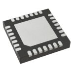 9FGL6251AP301NDGI8
The activity of extra discounts on wholesale prices is in full swing…
Please fill in your contact information and we will send you the latest wholesale price list.






