ChipApex | Global Electronic Components Supplier
9FGU0631CKLF
Search Product
Search Post
— IC芯片 | 连接器 | 传感器 | 被动器件 —
Search productSearch post
— IC芯片 | 连接器 | 传感器 | 被动器件 —
Consult the customer manager about the wholesale price.
consultation hotline:86-132-6715-2157
email:[email protected]
Contact the product manager for consultation. One-stop consultation is available.
Do you want a lower wholesale price? Please send us your inquiry and we will reply immediately.
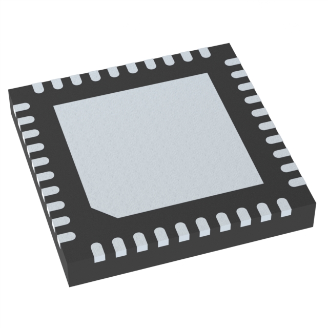
The Renesas Electronics 9FGU0631CKLF is a six-output clock buffer designed for PCI Express (PCIe) Gen1, Gen2, and Gen3 applications. Operating at a nominal 1.5 V supply voltage, this device functions as a PCIe clock generator with jitter attenuation capabilities. It features LP-HCSL outputs to reduce external component requirements. The component belongs to the 9FGU0631 series within the Clock & Timer ICs category. It is manufactured by Renesas Electronics Corporation and utilizes a surface-mount package configuration suitable for high-density board layouts.
The 9FGU0631CKLF is listed as obsolete or end-of-life by the manufacturer. Availability is restricted, and distributors may not stock this specific part number. Verification of current lifecycle status and alternative sourcing channels is required before procurement planning. Moisture sensitivity level details should be confirmed via the official datasheet prior to handling.
Select this component when designing for PCIe Gen1 through Gen3 interfaces requiring a single-source clock with jitter cleaning. Ensure the design supports the 1.5 V core voltage and LP-HCSL output swing. Verify that the six-output topology matches the target system's clock tree requirements. Consider the VFQFPN package dimensions for PCB footprint compatibility.
This part is a member of the Renesas IDT 1.5 V Ultra-Low-Power PCIe clock family. It shares architectural similarities with other devices in the 9FGU0631 series but is distinguished by its specific output count and packaging variant. The CKLF suffix typically denotes the commercial temperature range and tray packaging format within the product line.
Due to the obsolete status, direct substitutes are limited. Evaluate newer generations from the Renesas PCIe clock portfolio that support equivalent PCIe speeds. Cross-reference pinouts and electrical specifications carefully when considering legacy IDT parts or modern equivalents.
 9FGU0631CKLF
The activity of extra discounts on wholesale prices is in full swing…
Please fill in your contact information and we will send you the latest wholesale price list.