ChipApex | Global Electronic Components Supplier
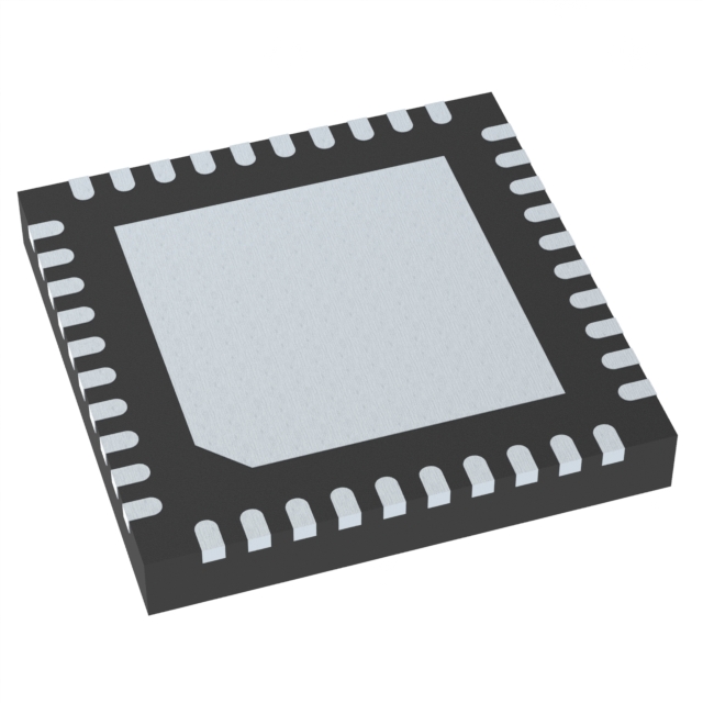
9FGU0631CKLFT
Search Product
Search Post
— IC芯片 | 连接器 | 传感器 | 被动器件 —
Search productSearch post
— IC芯片 | 连接器 | 传感器 | 被动器件 —
Consult the customer manager about the wholesale price.
consultation hotline:86-132-6715-2157
email:[email protected]
Contact the product manager for consultation. One-stop consultation is available.
Do you want a lower wholesale price? Please send us your inquiry and we will reply immediately.
The 9FGU0631CKLFT is a clock buffer manufactured by Renesas Electronics, designed for PCIe Gen1-2-3 applications. It features six outputs operating at a 1.5 V supply voltage. The device supports low-power HCSL (LP-HCSL) output signaling to reduce power consumption and board space requirements. It is housed in a surface-mount package suitable for high-density designs. The component operates within a specified temperature range and includes features for system stability and EMI reduction.
The 9FGU0631CKLFT is listed as obsolete or end-of-life by the manufacturer. Availability is limited to existing stock or third-party distributors. Verify moisture sensitivity level (MSL) and reflow soldering profiles before procurement. Check RoHS compliance status and ensure the specific suffix matches the required packaging type for production integration.
Select this component when a six-channel clock distribution solution is required for PCIe interfaces. Ensure the design utilizes 1.5 V logic levels compatible with LP-HCSL drivers. Compare against newer Renesas families if long-term supply assurance is critical. Verify that the input clock frequency and jitter specifications meet the target application's timing requirements.
This part belongs to the 9FGU0631 series of ultra-low-power PCIe clock buffers. It is related to other variants such as the 9FGU0831, which offers eight outputs. The CKLFT suffix typically denotes a tape-and-reel packaging format with specific thermal and mechanical characteristics defined by the manufacturer.
Direct replacements may include the 9FGU0831 for increased channel count or newer Renesas PCIe clock generators. Verify pin-to-pin compatibility and electrical parameter alignment before substitution.
 9FGU0631CKLFT
The activity of extra discounts on wholesale prices is in full swing…
Please fill in your contact information and we will send you the latest wholesale price list.