ChipApex | Global Electronic Components Supplier
9FGU0641AKLFT
Search Product
Search Post
— IC芯片 | 连接器 | 传感器 | 被动器件 —
Search productSearch post
— IC芯片 | 连接器 | 传感器 | 被动器件 —
Consult the customer manager about the wholesale price.
consultation hotline:86-132-6715-2157
email:[email protected]
Contact the product manager for consultation. One-stop consultation is available.
Do you want a lower wholesale price? Please send us your inquiry and we will reply immediately.
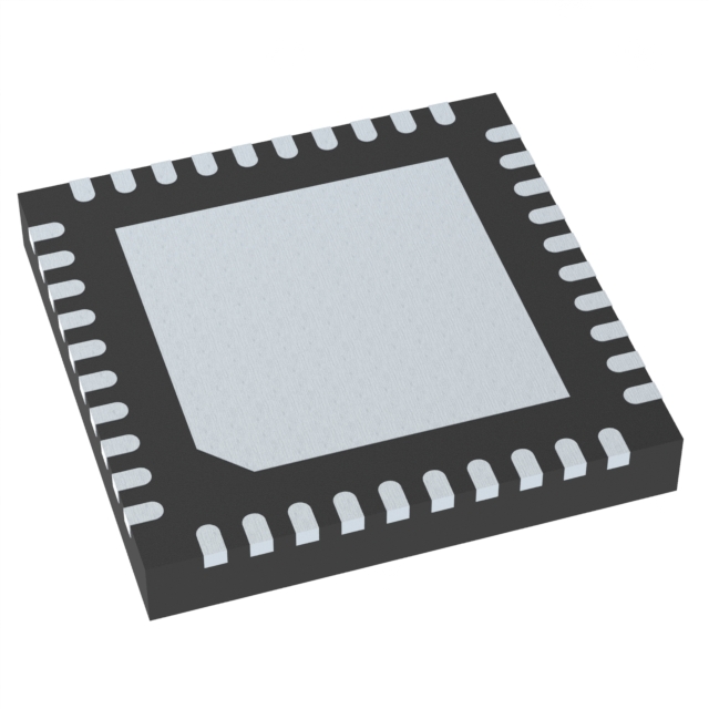
The 9FGU0641AKLFT is a clock generator from the Renesas 9FGU0841 family, designed for PCIe Gen1-2-3 applications. It features eight outputs operating at 1.5V with LP-HCSL signaling. The device supports a maximum output frequency of 100 MHz and accepts an input frequency up to 27 MHz. Typical power consumption is low, with an operating supply voltage of 1.5V. It utilizes a 40-pin VFQFPN package (5x5 mm) suitable for surface mount installation. The component operates within a temperature range of -40°C to +85°C and includes integrated terminations for direct connection to 100 ohm transmission lines.
Verify the specific output count and voltage level against the official datasheet, as the model number suggests an 8-output variant similar to the 9FGU0841, while some distributor listings may contain conflicting attributes. Confirm moisture sensitivity level and packaging details such as reel or cut tape availability directly with the manufacturer or authorized distributors before ordering.
Select this component when designing systems requiring multiple differential clock outputs for PCIe Gen1-2-3 interfaces with low power constraints. Ensure the design environment supports the 1.5V supply voltage and that the board layout accommodates the 5x5 mm 40-pin VFQFPN package. Verify compatibility with the required spread spectrum settings and SMBus address configurations for the target application.
This part belongs to the Renesas IDT SOC-Friendly Very-Low-Power PCIe clock family. It is related to the 9FGV0641 series but differs in output count and supply voltage. The product line is transitioning to SiTime, with documentation and support available through Renesas until the end of 2026.
Publicly confirmed substitute part numbers are not available in the provided source material. Consult the official datasheet for recommended alternatives or contact the manufacturer for cross-reference information.
 9FGU0641AKLFT
The activity of extra discounts on wholesale prices is in full swing…
Please fill in your contact information and we will send you the latest wholesale price list.