 ChipApex | Global Electronic Components Supplier
9FGV0231AKLF
Search Product
Search Post
— IC芯片 | 连接器 | 传感器 | 被动器件 —
Search productSearch post
— IC芯片 | 连接器 | 传感器 | 被动器件 —
Consult the customer manager about the wholesale price.
consultation hotline:86-132-6715-2157
email:[email protected]
Contact the product manager for consultation. One-stop consultation is available.
Do you want a lower wholesale price? Please send us your inquiry and we will reply immediately.
The Renesas 9FGV0231AKLF is a PCIe clock generator and fanout buffer IC designed for PCI Express Gen 1, 2, and 3 applications. It features an integrated PLL to generate up to three outputs from a single crystal input at frequencies up to 100 MHz. The device operates on a 1.8 V supply voltage with a range of 1.7 V to 1.9 V. It utilizes HCSL and LVCMOS output types and is housed in a 24-VFQFPN package with exposed pads. The component supports surface mount installation and functions within a commercial temperature range of 0°C to +70°C.
Verify the specific suffix 'AKLF' against the manufacturer's current datasheet to confirm pinout compatibility and RoHS status. Check for Product Change Notifications (PCNs) regarding package revisions or assembly site changes. Confirm moisture sensitivity level (MSL) handling requirements prior to soldering. Ensure the ordering quantity matches the manufacturer's standard packaging unit, which is typically 490 units per tray.
Select this component when a low-jitter, fixed-frequency PCIe clock source is required for Gen 1 through Gen 3 systems. It is suitable for designs needing one input and three outputs in a compact 24-pin QFN footprint. Consider the 1.8 V supply constraint and ensure the load capacitance matches the output drive requirements for HCSL or LVCMOS signaling. Verify that the 0°C to +70°C operating range meets the environmental specifications of the target application.
The 9FGV0231 series belongs to Renesas' PhiClock family of clock generators optimized for high-speed serial interfaces. This specific model provides a non-programmable solution for standard PCIe reference frequencies. It serves as a direct replacement for legacy clock buffers in motherboard and expansion card designs requiring precise timing alignment for PCIe lanes.
Cross-reference with the 9FGV0231AKLFT variant if tape-and-reel packaging is preferred over trays. Verify electrical equivalence with other 9FGV0231 variants before substitution, as differences may exist in output drive strength or package thermal characteristics.
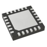 9FGV0231AKLF
The activity of extra discounts on wholesale prices is in full swing…
Please fill in your contact information and we will send you the latest wholesale price list.






