ChipApex | Global Electronic Components Supplier
9FGV0631CKILFT
Search Product
Search Post
— IC芯片 | 连接器 | 传感器 | 被动器件 —
Search productSearch post
— IC芯片 | 连接器 | 传感器 | 被动器件 —
Consult the customer manager about the wholesale price.
consultation hotline:86-132-6715-2157
email:[email protected]
Contact the product manager for consultation. One-stop consultation is available.
Do you want a lower wholesale price? Please send us your inquiry and we will reply immediately.
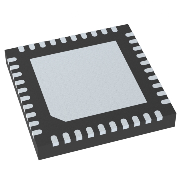
The Renesas 9FGV0631CKILFT is a PCIe clock generator and distribution IC designed for high-performance computing applications. It features a single circuit with a 1:6 input-to-output ratio, supporting differential LP-HCSL and LVCMOS outputs. The device accepts LVDS or crystal inputs and operates at frequencies up to 100MHz. Powered by a 1.7V to 1.9V supply, it functions within a -40°C to 85°C temperature range. Housed in a 40-VFQFPN (5x5) package with an exposed pad, this component integrates PLL functionality for precise clock generation and distribution.
Verify the specific ordering suffix against official Renesas documentation to confirm package type and material specifications. Ensure compatibility with required voltage levels and output configurations before procurement. Cross-reference datasheet revisions to confirm current manufacturing status and any potential product change notifications affecting the component.
Select this component when designing PCIe Gen 1 through Gen 6 interfaces requiring low-power clock distribution. Confirm that the 1.7V to 1.9V supply voltage aligns with the system design. Evaluate the need for integrated termination resistors to simplify PCB layout. Verify that the 100MHz maximum frequency meets the target application's timing requirements.
This part belongs to the Renesas PhiClock family of clock generators. It is specifically engineered for PCI Express compliance, offering flexible clocking architectures. The device supports multiple spread spectrum modes to minimize EMI, making it suitable for dense electronic designs where signal integrity is critical.
Consult official Renesas substitution guides for verified alternatives. Generic clock buffers may not support the specific PCIe architectures or integrated termination features required for direct replacement.
 9FGV0631CKILFT
The activity of extra discounts on wholesale prices is in full swing…
Please fill in your contact information and we will send you the latest wholesale price list.