 ChipApex | Global Electronic Components Supplier
9FGV0631CKLF
Search Product
Search Post
— IC芯片 | 连接器 | 传感器 | 被动器件 —
Search productSearch post
— IC芯片 | 连接器 | 传感器 | 被动器件 —
Consult the customer manager about the wholesale price.
consultation hotline:86-132-6715-2157
email:[email protected]
Contact the product manager for consultation. One-stop consultation is available.
Do you want a lower wholesale price? Please send us your inquiry and we will reply immediately.
The Renesas 9FGV0631CKLF is a single-circuit clock generator designed for PCI Express applications. It accepts LVDS or crystal inputs and provides HCSL and LVCMOS outputs with a 1:7 input-to-output ratio. The device operates within a supply voltage range of 1.7 V to 1.9 V and supports maximum frequencies up to 100 MHz. It is housed in a 40-VFQFPN package (5x5 mm) with an exposed pad, suitable for surface mount assembly. The component functions within an operating temperature range of 0°C to 70°C.
Verify the specific suffix 'CKLF' against official Renesas documentation to confirm the exact temperature grade and packaging details. Ensure compatibility with the required 1.7 V to 1.9 V power domain during design integration. Check for moisture sensitivity levels if storage conditions are critical.
Select this component when a single PLL circuit with seven outputs is required for PCIe designs. Confirm that the system environment stays within the 0°C to 70°C commercial temperature range. Verify that the available input sources match the supported LVDS or crystal configurations.
This part belongs to the Renesas clock generator family focused on PCI Express standards. It serves as a timing solution for systems requiring multiple clock domains derived from a single source. The 40-pin form factor allows for space-constrained board layouts.
Consult official Renesas cross-reference tools for verified substitutes. Ensure any replacement maintains the 1:7 ratio and compatible output signaling types.
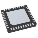 9FGV0631CKLF
The activity of extra discounts on wholesale prices is in full swing…
Please fill in your contact information and we will send you the latest wholesale price list.






