ChipApex | Global Electronic Components Supplier
9FGV0631CKLFT
Search Product
Search Post
— IC芯片 | 连接器 | 传感器 | 被动器件 —
Search productSearch post
— IC芯片 | 连接器 | 传感器 | 被动器件 —
Consult the customer manager about the wholesale price.
consultation hotline:86-132-6715-2157
email:[email protected]
Contact the product manager for consultation. One-stop consultation is available.
Do you want a lower wholesale price? Please send us your inquiry and we will reply immediately.
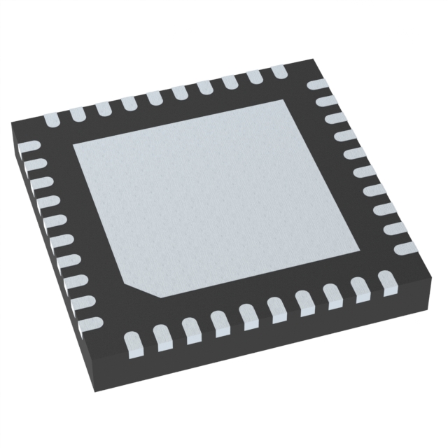
The Renesas 9FGV0631CKLFT is a clock generator IC designed for PCI Express applications. It features one circuit with a 1:6 input-to-output ratio, supporting LVDS or crystal inputs and LP-HCSL or LVCMOS outputs. The device operates at a maximum frequency of 100 MHz with a supply voltage range of 1.7 V to 1.9 V. It is housed in a 40-VFQFPN (5x5 mm) package with an exposed pad and functions within a temperature range of 0°C to 70°C.
Verify the operating temperature grade matches the design requirements, as this specific suffix indicates a commercial range of 0°C to 70°C. Confirm the package dimensions align with the PCB footprint, specifically the 40-VFQFPN exposed pad configuration. Ensure the supply voltage constraints are strictly maintained within the 1.7 V to 1.9 V window for proper operation.
Select this component when a dedicated PCIe clock generator with six outputs is required. It is suitable for designs needing LP-HCSL or LVCMOS output levels derived from LVDS or crystal sources. Consider the commercial temperature range limitation if the application environment exceeds 70°C. Verify that the 100 MHz maximum frequency meets the target bus speed requirements.
This part belongs to the Renesas clock generator family tailored for high-speed serial interfaces. It serves as a timing solution for systems requiring multiple synchronized clocks derived from a single reference source. The device integrates phase-locked loop functionality to minimize jitter and ensure signal integrity across the six output channels.
Check for updated revisions within the same series that may offer extended temperature ranges or alternative packaging options. Verify pin compatibility if substituting with other 40-pin VFQFPN clock generators. Ensure any replacement maintains the 1:6 ratio and supports the required input/output voltage levels.
 9FGV0631CKLFT
The activity of extra discounts on wholesale prices is in full swing…
Please fill in your contact information and we will send you the latest wholesale price list.