 ChipApex | Global Electronic Components Supplier
9FGV1001C001NBGI8
Search Product
Search Post
— IC芯片 | 连接器 | 传感器 | 被动器件 —
Search productSearch post
— IC芯片 | 连接器 | 传感器 | 被动器件 —
Consult the customer manager about the wholesale price.
consultation hotline:86-132-6715-2157
email:[email protected]
Contact the product manager for consultation. One-stop consultation is available.
Do you want a lower wholesale price? Please send us your inquiry and we will reply immediately.
The 9FGV1001C001NBGI8 is a programmable clock generator from the Renesas PhiClock family, designed for PCIe Gen1 through Gen5 applications. It operates within a temperature range of -40°C to +85°C and utilizes a VFQFPN-24 package measuring 4.0 x 4.0 x 0.8 mm. The device provides four non-spread-spectrum copies of a single output frequency and two copies of the crystal reference input. Key electrical parameters include a typical RMS phase jitter of 0.267 ps, an input frequency range of 25–25 MHz, and a core voltage of 3.3 V. Output frequencies are configurable at 50, 100, 125, or 156.25 MHz using LP-HCSL signaling.
Verify the specific suffix NBGI8 against the official datasheet to confirm the tray packaging quantity of 490 units and lead-free status. Confirm that the factory-configured OTP settings match the required output frequencies before procurement, as this is a pre-programmed device.
Select this component when four identical non-spread-spectrum clocks are required alongside two reference copies. Ensure the design supports LP-HCSL output levels at 3.3 V. Verify that the fixed factory configuration meets the target frequency specifications, as user reprogramming is not supported for this specific part number.
This part belongs to the 9FGV1001 series, which serves as a root part for various clock configurations. The NBGI8 suffix indicates a specific factory programming option packaged in trays, distinguishing it from reel-packaged variants like the NBGI8 or other pin-compatible models in the PhiClock family.
Direct replacements must share the same factory OTP configuration and package dimensions. Check for updated PCNs regarding assembly locations or label changes. Cross-reference with other 9FGV1001 variants only if the fixed output frequencies align exactly with the system requirements.
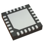 9FGV1001C001NBGI8
The activity of extra discounts on wholesale prices is in full swing…
Please fill in your contact information and we will send you the latest wholesale price list.






