ChipApex | Global Electronic Components Supplier
9FGV1001CQ505LTGI
Search Product
Search Post
— IC芯片 | 连接器 | 传感器 | 被动器件 —
Search productSearch post
— IC芯片 | 连接器 | 传感器 | 被动器件 —
Consult the customer manager about the wholesale price.
consultation hotline:86-132-6715-2157
email:[email protected]
Contact the product manager for consultation. One-stop consultation is available.
Do you want a lower wholesale price? Please send us your inquiry and we will reply immediately.
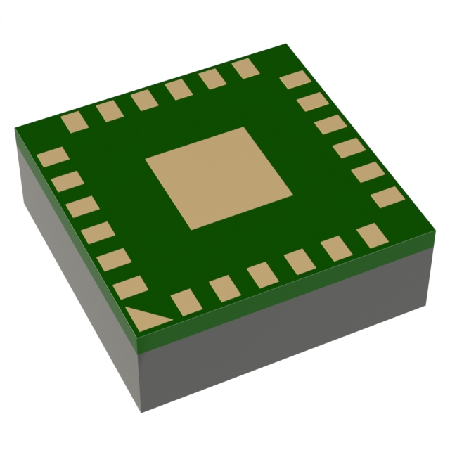
The 9FGV1001CQ505LTGI is a programmable clock generator from the Renesas PhiClock series. It features one circuit with a maximum frequency of 325MHz and a 1:6 input-to-output ratio. The device accepts HCSL, LVCMOS, LVDS, or crystal inputs and provides CML, HCSL, LP-HCSL, LVCMOS, LVDS, and LVPECL outputs. Operating on a 1.71V to 3.465V supply within -40°C to 85°C, it is housed in a 24-LFLGA (4x4mm) surface-mount package.
Verify the specific ordering suffix LTGI against official documentation to confirm package type and moisture sensitivity level. Ensure the selected variant matches the required output drive strength and pinout configuration for the target PCB layout. Cross-reference the manufacturer's latest datasheet for any updates regarding RoHS compliance status and recommended soldering profiles.
Select this component when a single-clock source must fan out to six distinct destinations with mixed signaling requirements. Confirm that the available input frequencies align with the internal PLL multiplication factors needed for the desired 325MHz maximum output. Evaluate the thermal performance of the 24-LFLGA package to ensure adequate heat dissipation under continuous operation at high frequencies.
This part belongs to the 9FGV1001 family of programmable clock generators designed for high-speed digital interfaces. The PhiClock series emphasizes low jitter performance and flexibility through factory-programmable configurations. The 24-LFLGA package offers a compact footprint suitable for dense board layouts in modern computing and networking equipment.
Consult the official Renesas replacement matrix for verified cross-references. Ensure any substitute maintains the 24-LFLGA footprint and compatible electrical characteristics for direct pin-to-pin integration without schematic modification.
 9FGV1001CQ505LTGI
The activity of extra discounts on wholesale prices is in full swing…
Please fill in your contact information and we will send you the latest wholesale price list.