 ChipApex | Global Electronic Components Supplier
9FGV1002B002NBGI
Search Product
Search Post
— IC芯片 | 连接器 | 传感器 | 被动器件 —
Search productSearch post
— IC芯片 | 连接器 | 传感器 | 被动器件 —
Consult the customer manager about the wholesale price.
consultation hotline:86-132-6715-2157
email:[email protected]
Contact the product manager for consultation. One-stop consultation is available.
Do you want a lower wholesale price? Please send us your inquiry and we will reply immediately.
The Renesas 9FGV1002B002NBGI is a programmable PhiClock™ generator designed for automotive and PCIe applications. It features four differential output pairs capable of generating spread-spectrum clock signals from a single input frequency, alongside two LVCMOS reference outputs. The device supports multiple I/O standards including LP-HCSL, LVDS, and LVCMOS, with individual supply voltage options for each output bank. Operating within an extended temperature range of -40°C to 85°C, it meets AEC-Q100 automotive qualification standards. The IC integrates a PLL for precise frequency synthesis and offers flexible configuration via hardware pins or I²C interface.
Verify the specific suffix 'B002' against the official 9FGV1002C datasheet addendum to confirm factory-configured parameters. Confirm package availability in 24-VFQFPN or 24-LGA formats as specified by the manufacturer's current production status. Ensure compliance with RoHS directives and check for any recent Product Change Notices affecting assembly locations or labeling.
Select this component when designing for PCIe Gen7 common clock requirements with strict jitter specifications. Ensure the design accommodates the required core voltage (1.8V/3.3V) and individual output supply voltages. Verify that the application utilizes the supported input types (Crystal, LVCMOS, LVDS, HCSL) and matches the desired output signaling standard (LP-HCSL, LVDS, or LVCMOS). Consider the I²C addressability if multiple devices are used on the same bus.
The 9FGV1002B002NBGI belongs to the Renesas PhiClock™ family of programmable clock generators. It shares the core architecture with the 9FGV1002 series but differs in factory-programmed OTP configurations. The 'NBGI' suffix typically denotes a specific tape-and-reel or tray packaging option and temperature grade variant within the broader 9FGV1002 product line.
Direct replacements include other 9FGV1002 variants with matching factory configurations. Verify pin compatibility between 24-VFQFPN and 24-LGA packages if swapping form factors. Cross-reference with 9FGV1006 series if additional output channels are required, ensuring electrical parameter alignment.
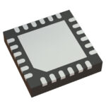 9FGV1002B002NBGI
The activity of extra discounts on wholesale prices is in full swing…
Please fill in your contact information and we will send you the latest wholesale price list.






